Terafab and the Orbital Foundry
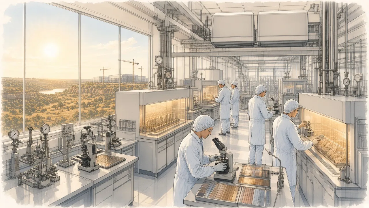
On the northern edge of Gigafactory Texas, on flat ground east of Austin where the Colorado River bends towards Bastrop, Tesla broke ground in April 2026 on a building it calls a research fab, the precursor to something far larger.[1] Ninety miles to the north-east, across the post-oak country of Grimes County, lies the farmland around Gibbons Creek Reservoir, where TeraFab AI, LLC has asked the Texas Comptroller to treat as many as four successive phases of semiconductor manufacturing as a single taxable project.[2] Between the two sites, in Bastrop, SpaceX says it is building a Gigasat Factory to turn out satellites whose only purpose is to compute in sunlight.[3]
The thread that joins these places is a bottleneck. Artificial intelligence is limited, its builders argue, less by algorithms than by chips, memory, packaging, electricity, land, cooling and permits. SpaceX’s own registration statement puts it plainly, stating that “the key constraints in the continued growth of AI are physical”.[4] Terafab is the answer that Tesla and SpaceX, with xAI and later Intel, announced in March 2026, an ambition to build “logic, memory, and advanced packaging all under one roof” and, eventually, to produce one terawatt of compute hardware a year, most of it destined for orbit.[5][6]
This special feature follows that ambition from its origins to its stated horizon. It begins with the missing layer in the companies’ industrial stack, the March announcement and its legal caveats, the research fab in Austin, the stack of Texas capital figures and the corridor from Taylor to Bastrop. It turns next to Gibbons Creek, the three chip families, Intel’s 14A process and its lithography, and the memory and packaging wall. The second half leaves the ground for the Starmind satellites, the thermodynamics of rejecting heat in vacuum, sunlit solar wings, radiation and leading-edge silicon, and the arithmetic of launch, before returning to the power, water and policy questions in Texas and to the clock against which the whole project will be judged. An interactive timeline at the end gathers the principal dates.
1. The missing physical layer
By the end of 2025 the companies that Elon Musk leads had assembled most of an industrial stack for artificial intelligence. Tesla designed its own inference processors and built the cars and humanoid robots that would carry them. SpaceX launched rockets, operated the Starlink constellation and was preparing Starship, a fully reusable vehicle intended to make mass in orbit cheap. xAI trained large language models on its Colossus clusters in Memphis. What none of them owned was the layer beneath everything else, the factories that turn sand-derived silicon wafers into transistors and memory cells.
That gap was named on Tesla’s fourth-quarter earnings call on 28 January 2026. Musk told analysts that chip production, meaning “enough AI logic and enough memory, enough RAM”, was likely to become the limit on growth “three or four years out”, and that even the “best case output” of strategic partners such as Samsung, TSMC and Micron would not suffice.[7] Tesla, he said, would have to build “a Tesla Terafab, a very big fab that includes logic, memory, and packaging, domestically”, partly “to ensure that we are protected against any geopolitical risks”.[7] He added that “there are no advanced memory fabs at scale in the United States. There are zero, literally zero.”[7] The chief financial officer, Vaibhav Taneja, noted that Tesla’s planned capital expenditure of more than $20 billion for 2026 did not include a semiconductor fab.[7]
The argument rested on growth rates rather than on any single shortage. The chip industry adds roughly a fifth more output a year, in Musk’s later estimate, while AI demand was growing faster, and every accelerator also needs memory, substrates and bonding capacity that are themselves scarce.[8] A company can design the best processor in the world and still be unable to ship it if those lines are booked by competitors.
In the weeks before the call, Musk had sketched a chip roadmap on X that already implied a factory of this kind. On 17 January he wrote that the AI5 design was almost done, that AI6 was at an early stage, and that Tesla was aiming for “a 9 month design cycle” through successive generations.[9] The next day he assigned roles to each generation, writing that “AI6 will be for Optimus and data centers” and that “AI7/Dojo3 will be space-based AI compute”.[10] Hours later he announced that Tesla would restart work on Dojo3, the training-chip line it had paused, and invited engineers to apply.[11]
A nine-month cadence is very fast by semiconductor standards. A new chip generation ordinarily takes two years or more from architecture to volume, much of it spent waiting for foundry slots, masks, test wafers and package qualification. A company that owns its own mask shop, wafer line and packaging floor can, in principle, compress that loop, and that recursive cycle became the technical centre of Terafab.
The second motive was destination. On 1 February Musk set out a scale ladder for chips in space, writing that AI5 and AI6 “will be fine for space at the low GW/year scale”, while AI7 and Dojo3 would serve deployments above ten gigawatts a year and AI8 above a hundred.[12] Two days earlier, on 30 January, a SpaceX affiliate had asked the US Federal Communications Commission to authorise a constellation of up to one million orbital data-centre satellites.[13] The demand Terafab was meant to meet lay largely above the atmosphere.
2. A terawatt announced in Austin
Musk had trailed the event a week earlier, writing that the project “launches in 7 days”. Terafab was formally launched on the evening of 21 March 2026, Central Time. A little before six in the evening in Texas, Musk posted that the project “will be done jointly by @SpaceX and @Tesla” with a livestream at around 8 p.m., and that “the goal is to produce over a TERAWATT of compute per year (logic, memory & packaging) with ~80% for space and ~20% for the ground”.[6] Shortly after eight, SpaceX posted “Announcing TERAFAB: the next step towards becoming a galactic civilization”, and Tesla carried the same announcement.[14] In a further post Musk explained the split, writing that “most must necessarily go to space, as US electricity is only 0.5TW”.[15]
That comparison can be checked. The United States consumes roughly four trillion kilowatt-hours of electricity a year, according to the Energy Information Administration, and dividing by the 8,760 hours in a year gives an average draw of about 0.46 terawatts. A terawatt of new computing hardware every year would, if all of it ran on the ground, add twice the country’s entire average electrical load annually.
The talk itself, recorded and posted to YouTube as “The Largest Chip Manufacturing Facility Ever”, was more concrete than the slogans.[16] Musk said that all existing fabs on Earth amounted to “only about 2% of what we need” for the terawatt goal, and summed up the logic: “We either build the Terafab, or we don’t have the chips, and we need the chips, so we build the Terafab.”[16] He described an “advanced technology fab” in Austin containing “all of the equipment necessary to make a chip of any kind”, together with mask making, so that “in a single building we can create a lithography mask, make the chip, test the chip, make another mask and have an incredibly fast recursive loop”.[16]
The space arithmetic was set out in the same talk. Reaching a terawatt of compute a year would require launching “about 10 million tons to orbit per year” at “100 kilowatts per ton” of satellite.[16] The Terafab website repeats the figure among its demand drivers, alongside one billion Optimus robots and more than a terawatt of solar power.[5] The chapter on launch returns to what that identity requires.
The rhetoric was civilisational. The website frames Terafab within the Kardashev scale, the Soviet astronomer Nikolai Kardashev’s 1964 classification of civilisations by the energy they command, and states the aspiration “to be a galactic civilization”.[5] The same language appears in SpaceX’s FCC application, which the Commission’s Space Bureau quoted as describing the orbital constellation as a “first step towards becoming a Kardashev II-level civilization – one that can harness the Sun’s full power”.[13] In July SpaceX tied the factory and the constellation together, describing Starmind and Terafab as “a step toward a Kardashev Type II civilization”.[17]
On 22 March, the day after the launch, Musk added two structural clarifications. The Austin building, he wrote, was “just the little advanced technology fab, where we will be iterating on chip designs”, because “we couldn’t possibly fit the Terafab on the GigaTexas campus”; the full plant “needs thousands of acres and over 10GW of power at full scale”.[18] He also wrote that Terafab would “technically be two fabs, each making only one chip design”, and that without it the companies would be “stuck at the ~20% chip/memory output growth per year of the current industry”.[8] Accounts differ on the hall in which the talk was given, and the record does not settle the point.
3. The framework and its caveats
Two months after the livestream, Terafab acquired a legal definition. SpaceX’s registration statement on Form S-1, filed on 20 May 2026, states that “‘Terafab’ refers to a chip manufacturing initiative with a long-term goal of producing one terawatt of compute hardware each year”.[4] The final prospectus, filed on 12 June ahead of the company’s listing, carries the same language.[19] Unlike a post on X, a prospectus carries legal liability for the issuer and its directors.
Terafab would “vertically integrate across the design of lithography masks, fabrication of logic and memory chips, and design of advanced packaging in a single closed-loop plant”, so that “rapid testing and iterations” could improve chip design and scale manufacturing faster.[19] It would support “two kinds of chips—one type optimized for terrestrial edge and inference to be used primarily in Tesla’s Optimus robots and vehicles, and another type optimized for the space environment to be used in our orbital compute infrastructure”.[19]
The same document is also the most important caveat in the public record. SpaceX and Tesla had agreed only “a general framework for the future development of Terafab”.[19] “Any specific projects undertaken pursuant to this framework will be subject to separate negotiations and agreements (including any development timelines, milestones and capital expenditures) and have not yet been determined.”[19] Among the risk factors, the company warns that “there can be no assurance that we will be able to achieve our objectives with respect to Terafab within the expected timeframes, or at all”, and that “neither Tesla nor Intel are obligated to remain a part of the project, and we may not enter into any such definitive agreements”.[19]
Read together, these sentences describe a project real in intent and early in substance. The terawatt is a long-term goal; the agreements that would fix who pays, who owns the intellectual property and who operates which building were, as of June 2026, still to be negotiated. The prospectus also expects SpaceX to “continue sourcing a significant portion” of its compute hardware from third-party suppliers, which places Terafab beside, not instead of, the merchant chip market.[19] The Texas filings and equipment reports that follow should be measured against that baseline.
Intel’s role illustrates the point. On 7 April 2026 Intel announced that it was “proud to join the Terafab project with @SpaceX, @xAI, and @Tesla to help refactor silicon fab technology”, citing its ability “to design, fabricate, and package ultra-high-performance chips at scale”.[20] Musk replied that he was “looking forward to working with Intel on the Terafab”.[21] Yet the prospectus filed six weeks later explicitly allowed for Intel’s departure, and in October Musk wrote that the companies “will build and run the fab”, adding that TSMC might at most sublease part of it.[22] The honest reading is a process-technology and packaging partnership whose definitive terms have not been published.
Even the name is contested. TERA-print, a small nanofabrication company in Skokie, Illinois, associated with the Northwestern University chemist Chad Mirkin, has for more than a decade sold desktop beam-pen lithography instruments under the mark TERA-FAB, registered with the US Patent and Trademark Office in 2021.[23] Tesla filed three trademark applications for the Terafab name on 18 May 2026; TERA-print sent a cease-and-desist letter on 23 May and threatened suit in June.[24] On 15 September Tesla, SpaceX and SpaceXAI asked the federal court in Austin for a declaratory judgment that their use does not infringe, in a case that remained open into November.[24][25]
The complaint is itself a useful primary source. It recites the 21 March announcement, the one-terawatt goal and the plan to integrate “chip design and manufacturing, logic, memory, and packaging under one roof”, with “initial testing and ramp-up in Austin, Texas”.[24]
4. The research fab at Giga Texas
The first Terafab building is not a megafab. It is a pilot line on the North Campus of Gigafactory Texas, where Tesla says it broke ground in April 2026 on “our research fab”, which it calls “the precursor to Terafab”.[1] On the first-quarter earnings call on 22 April, Musk gave its only numerical description so far. It would be “probably a $3 billion-ish initiative, and capable of maybe a few thousand wafers per month”, built “to try out ideas”, including “some new physics we’d like to test out”.[26] A few thousand wafer starts a month, he explained, is the scale needed “to make sure that a production process is sound”.[26]
Those figures place the building in a familiar category. Leading-edge chipmakers have long operated development lines, at Intel’s Oregon campus or in research consortia whose agendas are mapped by the International Roadmap for Devices and Systems, where new transistor structures, materials and lithography steps are proven before transfer to high-volume plants. What is unusual in Austin is the stated scope. The research fab is meant to do “memory, logic, everything in the same place, including mask”, so that a design can move from layout to reticle to wafer to test without leaving the building.[26] Musk’s ambition, set out the day after the launch, was a line able to produce new iterations of a design with less than a seven-day lag, allowing engineers to try “high risk, high return ideas”.[8]
Normally, masks come from specialist suppliers, wafers from a foundry shared with dozens of customers, and packaging from yet another company, often on another continent, and each hand-off adds weeks. Pulling them under one roof is meant to make silicon iterate more like software.
In the metrology bays of any modern fab, technicians in hooded gowns load wafers into scanning electron microscopes and optical overlay tools, checking whether the lines printed by lithography have landed within a few nanometres of where they should be. Ellipsometers measure film thicknesses, defect-inspection tools from companies such as KLA scan for particles, and electrical test stations probe simple structures to learn whether a new process step has changed transistor leakage.
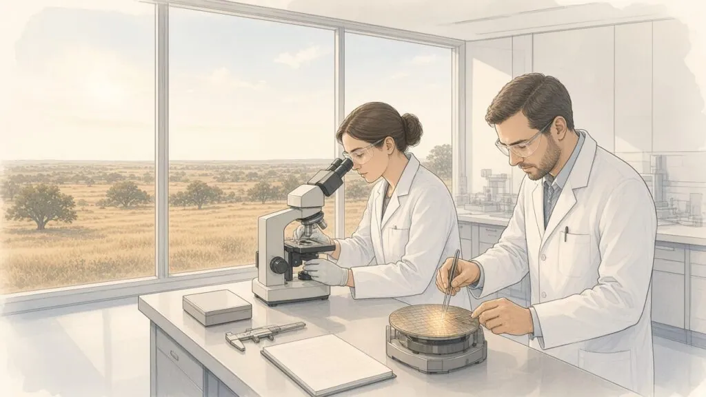
The first product target is correspondingly modest. On a SpaceX conference call around 20 October 2026, Musk was reported as saying that the internal aim was a first functional SRAM test chip at the Austin facility in roughly May or June 2027, and he described the overall schedule as “insanely fast”.[27] Static random-access memory arrays are the classic first vehicle for a new process because they are dense, regular and unforgiving. A large SRAM block exposes defects, variability and leakage quickly, and its yield is a sensitive measure of whether the line works. It is also a standard canary for radiation testing.
Tesla’s first-quarter update, filed with the US Securities and Exchange Commission, describes the arrangement in its own words. The partnership with SpaceX “aims to build the largest chip fab ever”, and “this begins with the Tesla-owned Research Fab on our Gigafactory Texas campus”.[28] On the call, Musk divided the labour plainly: “Tesla’s doing the research fab, SpaceX is doing the initial part of the large scale Terafab, and then we’ve got to figure out the rest.”[26] The boundary between them remained subject to later agreements and the review of independent directors.[26]
The research fab is not counted in the Texas incentive filings for the volume campus, and its roughly $3 billion is a separate figure from any of the larger numbers that follow.[26] It is where Terafab’s central claim, that a closed-loop factory can learn faster than the merchant industry, will first meet wafers.
5. A stack of Texas numbers
Public discussion of Terafab’s cost has swung between $3 billion, $16.8 billion, $55 billion, $119 billion and “over a trillion dollars”. All of these figures are real, but they measure different things and carry very different legal weight, and they are best read as a stack, from binding obligation to conditional remark.
The first figure to appear in an official Texas document was in a public notice dated 4 May 2026, issued ahead of a Grimes County hearing on 3 June. Space Exploration Technologies Corp. proposed a “multi-phase, next-generation, vertically integrated semiconductor manufacturing and advanced computing fabrication facility” at the Gibbons Creek Reservoir, with “estimated capital investment for the initial phases” of $55 billion and “an estimated total capital investment (if additional phases are constructed) of $119 billion”.[29] Those numbers are the applicant’s own description, not a commitment.
From 8 June, TeraFab AI, LLC filed eight applications under the Jobs, Energy, Technology and Innovation Act, Texas’s school-district property-tax limitation programme, four with Anderson-Shiro Consolidated Independent School District and four with Iola Independent School District.[2] The Phase 1 placement-in-service schedules give the exact source of the figure later used by the state. Anderson-Shiro’s application lists $10,366,217,000 of eligible investment over 2026 to 2028, and Iola’s lists $6,434,783,000, together $16,801,000,000.[30][31] When Tesla confirmed on 6 August that “Terafab will be built in Grimes County, Texas”, the state’s announcement, as reported at the time, described a first phase of more than $16.8 billion, matching the sum of the two schedules.[1][30]
| Figure | Amount | What it measures | Legal weight |
|---|---|---|---|
| Austin research fab | About $3 billion | Musk estimate for the Giga Texas pilot line, April 2026 | Indicative, outside the Grimes filings |
| County minimum | $5 billion by 2030 and 1,800 jobs by 2035 | Chapter 312 abatement for Grimes County | Binding, as reported from the signed agreement |
| JETI Phase 1 | $16.801 billion, 2026 to 2028 | Anderson-Shiro $10.366 billion plus Iola $6.435 billion | Eligible investment under a tax limitation |
| County notice | $55 billion | Applicant’s description of the initial phases, May 2026 | Descriptive |
| JETI four phases | About $119.39 billion, to 2036 | Eight applications, each phase optional | Eligible investment, phases at the applicant’s discretion |
| Prospectus | None stated | General framework between SpaceX and Tesla | Specific projects not yet determined |
| Long term | Over $1 trillion | Musk, conditional on a terawatt a year of silicon | Personal remark |
The Comptroller’s table of current agreements lists all eight applications at a 50 per cent limitation, in rounded amounts that total about $120 billion over four phases running to 2036.[2] Summing the underlying applications gives about $73.66 billion in Anderson-Shiro and $45.73 billion in Iola, or $119.39 billion, the figure behind the May notice’s $119 billion.[32] The Anderson-Shiro project description itself says that total capital “is expected to range between $55 billion and $119 billion for initial phases, with long-term expansion potential significantly exceeding this level”, and states that each phase “would be independently capable of manufacturing semiconductors”, after which the applicant “would then determine whether to proceed”.[30]
The binding numbers are far smaller. Reporting on the signed county agreement, approved on 3 June under Chapter 312 of the Tax Code and accompanied by an economic development agreement under Chapter 381 of the Local Government Code, found a contractual minimum investment of $5 billion by 31 December 2030 and 1,800 full-time-equivalent jobs by 31 December 2035, in exchange for a ten-year full abatement on buildings and equipment from 2027 to 2036.[33] The company may terminate on thirty days’ notice.[33]
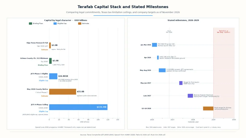
Job figures form a similar stack. The JETI statute requires as few as ten jobs per application, the consultants’ impact tables for Phase 1 show 617 direct operating jobs in Anderson-Shiro and 383 in Iola from 2029, the county agreement fixes 1,800 by 2035, and the state’s announcement, as widely reported but not retrieved for this essay from the governor’s website, spoke of 3,000.[2][30][31][33] Above all of these sit two remarks of a different kind. SpaceX’s prospectus commits no capital at all, describing only a framework.[19] And on 29 August Musk wrote that “Terafab will be over a trillion dollars long-term if it achieves a terawatt/year of silicon”.[34] An account that quotes only “$119 billion and 3,000 jobs” omits the conditions attached to both.
6. From Taylor to Bastrop
Terafab is usually described as two sites, but its footprint in central Texas involves at least four. The research fab sits at Giga Texas in Austin. The volume campus is planned for Grimes County. SpaceX’s Gigasat Factory in Bastrop, east of Austin, would build the satellites that are meant to consume most of the output.[3] And north-east of Austin, at Taylor, Samsung’s foundry is one of two merchant plants already contracted to make Tesla’s next inference chip.[7]
Taylor and its counterpart in Phoenix, TSMC Arizona, belong to the wave of American fab construction that followed the CHIPS and Science Act of 2022, the federal programme of grants, loans and tax credits that the Congressional Research Service has catalogued project by project.[35] On the January call Musk said that Tesla already had “chip supply deals with TSMC in Arizona and Samsung in Texas”.[7] Industry reporting in 2025 described the Samsung agreement as worth about $16.5 billion over eight years, a figure this essay attributes to reporting rather than to any company filing.
Terafab therefore enters a busy corridor, beside a merchant foundry at Taylor. The JETI applications add a fifth element to the Grimes campus itself, a “space compute test facility”, alongside power generation, which suggests that some qualification of orbital hardware is planned close to the wafers.[30] Austin, Taylor, Bastrop and the Gibbons Creek site lie within roughly a hundred miles of one another, joined by state highways maintained by TxDOT that will carry the construction traffic.
The flow through this system can be traced from sand to orbit. Masks and wafers are made at the research fab and, later, at Grimes County. Logic and memory dies are packaged, tested and either built into Tesla vehicles and Optimus robots on the ground or shipped to Bastrop for integration into satellite compute modules. From there the satellites travel to launch sites, reach sun-synchronous orbit, and return results to Earth over laser links through Starlink.[3] Each arrow in that chain is a separate industrial problem with its own regulator.
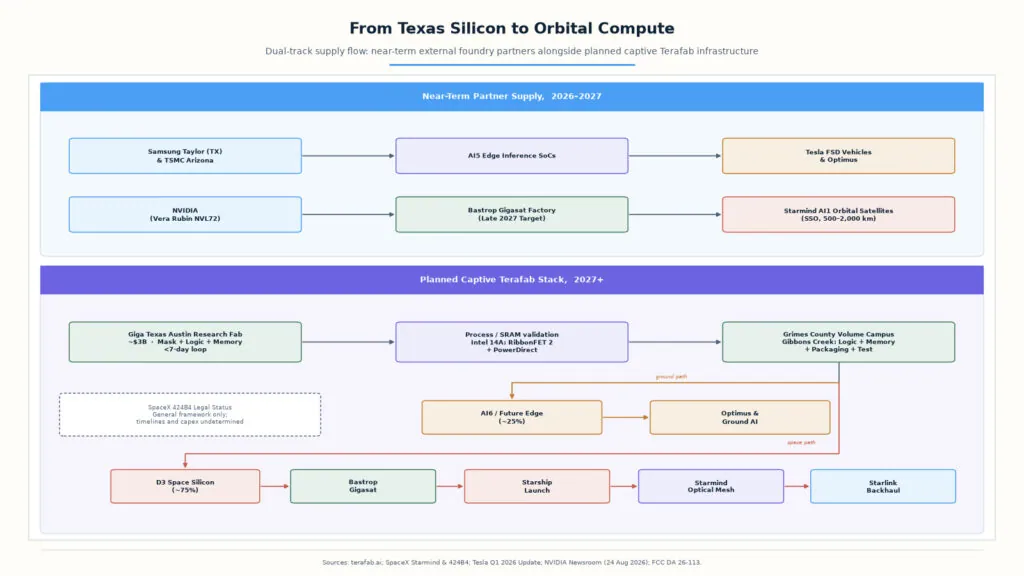
The orbital end of the chain does not depend on Terafab at the outset. SpaceX’s Starmind page describes the satellite architecture as “AI chip vendor agnostic” and modular, and NVIDIA announced on 24 August 2026 that SpaceXAI’s “planned first-generation Starmind AI satellite will be based on the optimized NVIDIA Vera Rubin NVL72 rack-scale system”.[3][36] The near-term silicon for the cars is likewise made by Samsung and TSMC. Terafab is intended to take over these flows progressively, not to supply the first products of either programme.
This sequencing is what the prospectus describes when it calls Terafab “complementary” to third-party supply.[19] It is also why the share of Terafab output assigned to space has moved. In March Musk spoke of about 80 per cent for space and 20 per cent for the ground.[6] On 6 August he offered a “very approximate guess” of about 25 per cent for Tesla Optimus and 75 per cent for AI spacecraft.[37] The allocation of a factory not yet built remains a forecast.
Bastrop County, home to the city of Bastrop along the Colorado River, had already received a $17.3 million grant from the Texas Semiconductor Innovation Fund in March 2025 for a SpaceX expansion there, a separate and much smaller instrument that should not be added to Terafab’s totals. The volume campus, by contrast, would be placed in a county whose largest industrial landmark for more than three decades was a power station, beside a reservoir built to cool it.
7. Surveyors at Gibbons Creek
Gibbons Creek Reservoir lies in eastern Grimes County, between the small towns of Anderson and Iola and about twenty miles east of College Station, home of Texas A&M University. The lake was impounded in the early 1980s to supply cooling water to a coal-fired power station that has since been retired, and the land around it is a patchwork of pasture, woodland and old industrial ground. It offers what large factories need and seldom find near a city, flat terrain, water, transmission corridors and room to grow.
The JETI applications show how the site was assembled. Anderson-Shiro’s Phase 1 filing lists dozens of tracts around Gibbons Creek Road and State Highway 30, among them a single parcel of 1,987.1 acres, together with many smaller holdings of a few acres each.[30] Iola’s filing covers the remainder of the campus on the other side of the district line.[31] The parcel list is consistent with Musk’s remark that the full plant “needs thousands of acres”, although the total acreage should be summed from both districts’ schedules before it is quoted as a single figure.[18][30]
The Anderson-Shiro project description calls the campus a “next-generation, vertically integrated semiconductor manufacturing and advanced computing fabrication, packaging, and deployment facility” that would consolidate “integrated circuit design, photomask generation, wafer fabrication, advanced packaging, and system-level integration, with supporting power generation and a space compute test facility”.[30] The list of eligible property runs from fab buildings, clean rooms and sub-fabs to a central utility plant, substations, water treatment and recycling, industrial waste treatment, on-site and backup generation, lithography, etch and deposition tools, automated material-handling robotics, dry cooler arrays and utility-scale battery storage.[30]
The filings also state why the site is in Texas. A JETI limitation is described as a “compelling factor” in the location decision, and school-district maintenance-and-operations property tax as “the single largest recurring cost differential between Texas and competing jurisdictions”.[30] They anticipate “leading-edge semiconductor process technologies, including sub-2 nanometer class nodes”, and record that “initial development activities, including prototype fabrication and process validation, are currently underway in Texas”.[30]
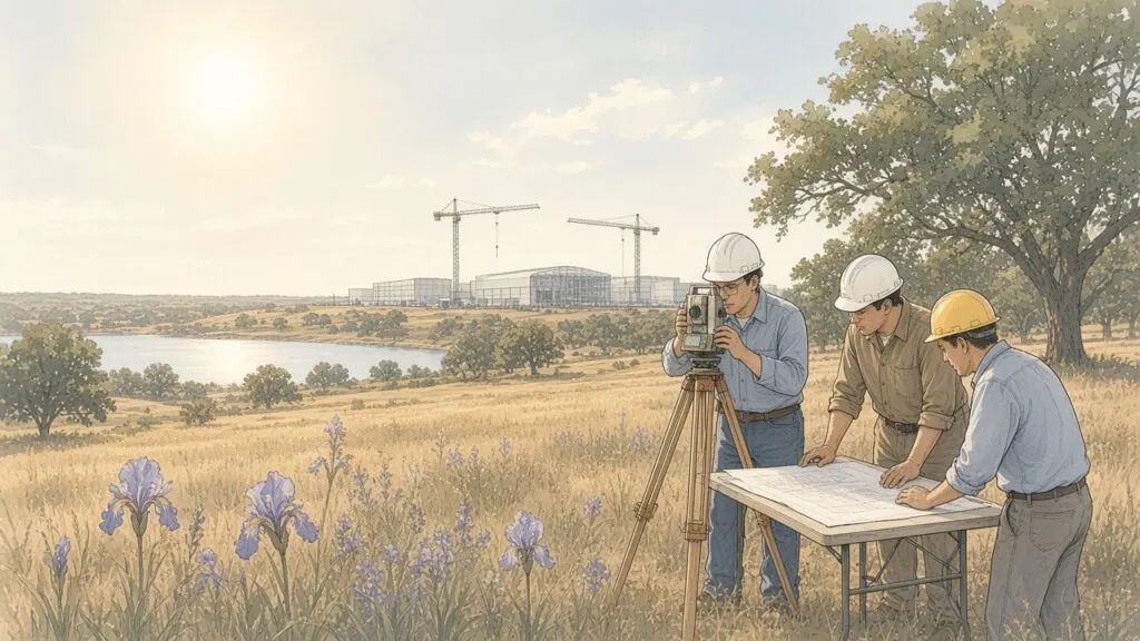
Before any of this can rise, the ground must be measured. Survey crews working such a site set out control points with satellite receivers and total stations at first light, before the heat shimmers the line of sight, and geotechnical teams drill boreholes to learn how the clay and sand beneath will bear a building that must not vibrate. Lithography scanners tolerate almost no floor movement, so fab foundations are thick, isolated slabs.
Local reaction has been divided. At the Commissioners Court hearing on 3 June 2026, residents raised concerns about water, roads and the rural character of the county, while supporters pointed to jobs and tax base.[33] The court approved a reinvestment zone, the abatement and the economic development agreement the same day.[33] A citizens’ group, Grimes County Citizens for Responsible Development, later published a combined summary of the eight JETI applications, a useful reading aid that should always be checked against the Comptroller’s own documents.[32] The engineering press traced how the eight applications fitted into a four-phase buildout.[38]
The reservoir is both a resource and a political object. Leading-edge fabs consume large volumes of ultrapure water, much of it recycled, and the Phase 1 text lists water treatment and recycling without publishing a daily volume.[30] Any water drawn from the Brazos River basin, in which Gibbons Creek lies, falls within a planning system run by the Texas Water Development Board and regional authorities such as the Brazos River Authority. Those numbers, when they are disclosed, will matter more to the county than the headline capital figures.
8. Three chip families
The Terafab website lists three product families and leaves room for more. AI5 is “Powering FSD & Tesla Optimus”, AI6 is “Powering Tesla Optimus”, D3 is “Powering Space”, and a fourth entry reads simply “and Beyond”.[5] Behind those labels lie three different supply arrangements, which public discussion often collapses into one.
AI5 is Tesla’s next-generation inference system-on-chip for Full Self-Driving and Optimus, with data-centre use also planned. Tesla’s first-quarter update records that it “completed the final chip design” of AI5 in April 2026, and near-term wafers are planned at Samsung Taylor and TSMC Arizona rather than at Terafab.[28][7] Musk’s most quoted description came on 19 January 2026, when he wrote that AI5 would be “roughly Hopper class as single SoC and Blackwell as dual, but it costs peanuts and uses much less power”, comparing it with two generations of NVIDIA data-centre accelerators.[39] That “peanuts” line is a claim about the cost and power of a chip, not about launch prices.
Over 2025 and 2026 Musk spoke variously of very large multiples over the current AI4 computer on some metrics, of about five times the useful compute of a dual-chip AI4 board, and of roughly eight times the compute, nine times the memory and five times the bandwidth. Each may be true of a particular benchmark at a particular design freeze, and reducing them to a single factor hides where the gains come from.
AI6 is less defined. Musk wrote on 18 January that “AI6 will be for Optimus and data centers”, and on the January call said that it would “aspirationally” follow AI5 “in under a year” as “yet another big leap”.[10][7] It is listed on the Terafab website as a Terafab output, but no primary source yet assigns it a process node, a foundry split or a start date at Grimes County.[5] A fab built for rapid iteration needs designs that iterate.[9]
| Family | Stated role | Near-term manufacture | Terafab role | Status |
|---|---|---|---|---|
| AI4 | Current FSD computer, also in Tesla data centres | Merchant foundry | None | In service |
| AI5 | FSD and Optimus inference, data-centre use | Samsung Taylor and TSMC Arizona | Listed Terafab product, later in-house | Final design April 2026 |
| AI6 | Optimus and data centres | Not specified | Listed Terafab product | Targeted within a year of AI5 |
| D3, with AI7 or Dojo3 | Space computing | Not specified | Space-optimised Terafab product | No published datasheet |
| Vera Rubin NVL72, optimised | First-generation Starmind AI1 | NVIDIA supply chain | None | Announced August 2026 |
D3 is the official name for the space chip, but it is related to, rather than identical with, other labels Musk has used. Tesla’s earlier Dojo line began with the D1 training chip. On 18 January Musk said that work would restart on Dojo3 and that “AI7/Dojo3 will be space-based AI compute”, and on 1 February he placed AI7 and Dojo3 at the scale of more than ten gigawatts a year in orbit, with AI8 beyond a hundred.[11][10][12] The website’s D3 is best read as the product-family name for the space part and AI7 or Dojo3 as Musk’s earlier designation, without assuming a one-to-one match of mask sets.
Secondary reports have described D3 as a chiplet design using 2.5D and 3D packaging with stacked high-bandwidth memory, radiation-tolerant and higher in power than terrestrial parts. None of it appears in the prospectus, the JETI text or the official website. What the prospectus does state is the principle, two kinds of chip, one “optimized for terrestrial edge and inference” and another “optimized for the space environment”.[19]
The first flight hardware is, in any case, not D3. NVIDIA’s August announcement states that the first-generation Starmind satellite will use an optimised Vera Rubin NVL72 system, extending into orbit the rack-scale architecture that NVIDIA’s GB200 NVL72 established on the ground.[36] In March NVIDIA had already launched a Space-1 Vera Rubin Module said to deliver “up to 25 times more AI compute” than an H100 for space-based inference, with launch partners that did not yet include SpaceX.[40]
9. Intel 14A and the light that draws it
On the April call Musk made the first on-the-record choice of process. “We plan to use Intel’s 14A process, which is state-of-the-art and in fact not yet totally complete,” he said, adding that “by the time Terafab scales up, 14A will be probably fairly mature or ready for prime time”.[26] Tesla and SpaceX were choosing a node not yet in high-volume production, expecting node and factory to mature together.
Intel’s foundry process page describes 14A as “a generational advancement” built on two technologies.[41] The first is RibbonFET 2, Intel’s second-generation gate-all-around transistor, in which the channel is a stack of thin horizontal silicon ribbons wrapped on all sides by the gate. The second is PowerDirect, a backside power-delivery scheme in which the wiring that carries current to the transistors is moved beneath the silicon, leaving the front-side metal layers free for signals.[41] Intel claims, on internal analysis, 15 to 20 per cent more performance at the same power, or 25 to 35 per cent lower power at the same performance, and up to 30 per cent greater density than its 18A node.[41]
Ribbons and the back of the wafer
Both ideas answer old problems. As transistors shrank, the fin-shaped channels of FinFETs became hard to control, since the gate touched them on only three sides and current leaked through the fourth. Wrapping the gate fully around stacked ribbons restores control. Backside power addresses a separate limit. In a conventional chip, power and signal wires compete for the same crowded layers above the transistors, and the voltage drop along thin power lines wastes energy and constrains clock speed. Intel’s 18A introduced the first versions, RibbonFET and PowerVia, and 14A refines both.[41]
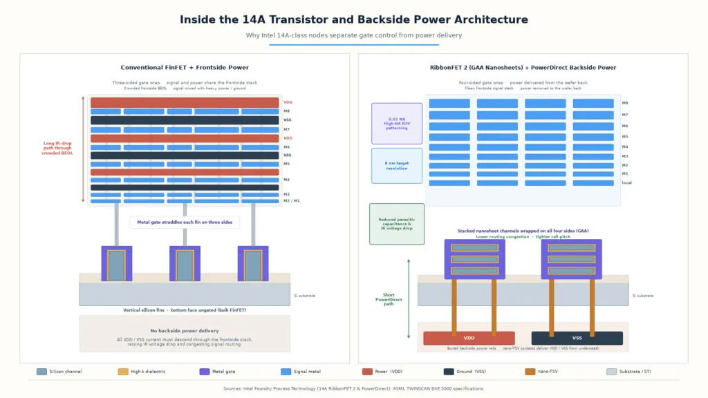
For dense AI accelerators, which draw hundreds of amperes at low voltage, backside power is particularly attractive. It shortens the path from the package to the transistors and reduces the resistive loss known as IR drop. It also creates a new surface, the thinned back of the wafer, which becomes a new reliability question for anyone stacking dies or adding shielding for space.
Thirteen and a half nanometres
The patterns for such transistors are drawn with extreme ultraviolet light at a wavelength of 13.5 nanometres. The lithography principle is that the smallest printable feature scales with wavelength divided by the numerical aperture of the optics. The current generation of EUV systems uses an aperture of 0.33. ASML’s TWINSCAN EXE:5000, the first High-NA tool, raises it to 0.55, giving a resolution of 8 nanometres, features 1.7 times smaller and transistor densities 2.9 times higher than the earlier systems, with 40 per cent more imaging contrast.[42] Its anamorphic optics keep standard mask sizes but halve the exposure field, so the stages must move faster to hold throughput.[42]
Intel has been the lead customer for High-NA, installing early tools at its Oregon development fab and working with ASML through 2026 on mask, resist and process readiness.[43] The purpose is to print the finest layers in a single exposure rather than several, saving steps and overlay error. ASML ships EUV scanners, each built around a laser-driven tin-plasma light source, in quantities of a few dozen a year, and High-NA units far fewer.
That scarcity is the practical limit behind the schedule. Musk was reported in October as saying that critical suppliers, including ASML, were expediting shipments.[27] A 2028 volume start on 14A would come early in the node’s life, while yields are still climbing. The bet, in effect, is that a single-product line run by its own customer can climb that curve faster than a foundry serving many customers, a thesis that the research fab exists to test.
10. Memory and the packaging wall
Musk has said more than once that memory may be a tighter constraint than logic.[7] In April he said that the rate at which the industry was growing, “in logic but even more so in memory”, meant that “we just anticipate hitting the wall if we don’t make chips ourselves”.[26] He added that Terafab was “not some sort of mechanism to generate leverage over our chip suppliers”, and that the motive was quantity.[26]
The reason is architectural. A modern AI accelerator spends much of its time waiting for data, and its performance depends on how many bytes per second can be moved between memory and the arithmetic units. The industry’s answer is high-bandwidth memory, stacks of DRAM dies joined by thousands of vertical through-silicon vias and placed beside the processor on a silicon interposer or bridge. HBM is made by only a handful of companies, among them SK hynix, Samsung and Micron, under standards set by JEDEC, and its supply has been as tight as that of leading-edge logic.
Packaging is the second wall. The interposers and bridges that connect logic and HBM, such as TSMC’s CoWoS family and Intel’s EMIB and Foveros technologies, require their own clean rooms, lithography and bonding tools. Each HBM stack dissipates tens of watts within a tight junction-temperature window, and bonding yields, underfill and warpage are recurring problems. Die-to-die standards such as UCIe aim to let chiplets from different processes be combined.
Terafab’s response is to place logic, memory and packaging on one campus, which almost no existing leading-edge site does. Memory and logic use different process families, different equipment mixes and different yield cultures. Intel’s 14A is a logic process, and no source reviewed here has said what memory process, or whose, would sit beside it.[41]
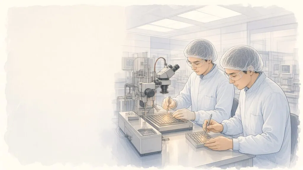
On a packaging floor, the work is closer to precision assembly than to chemistry. Operators feed trays of known-good dies into thermocompression bonders that align them to the interposer within a micrometre, dispense underfill, and cure the assemblies in ovens. At probe stations, needle cards touch the pads of bare dies before bonding, so that a bad die is discarded rather than buried in an expensive package. Every point of yield lost here multiplies across every chiplet in the assembly.
The most striking memory figure in circulation is not an official one. On 9 November 2026 the Korean newspaper Financial News reported that Terafab’s procurement team had told Japanese toolmakers it was seeking about one million wafers a month after 2032, about 700,000 of them for memory and more than 300,000 for logic, and that some suppliers had been asked to deliver within months.[44] TrendForce and Tom’s Hardware followed, noting that 700,000 memory wafers a month would rival the estimated DRAM capacity of Samsung itself.[45][46]
Those figures should be read with care. They come from procurement-channel reporting, not from a Tesla, SpaceX or JETI document. “Memory” in such a report need not mean DRAM alone, and a mix including NAND flash would change any comparison. A leading-edge logic fab is usually discussed in terms of tens of thousands of wafer starts a month per building, so one million a month on a single campus would be without precedent. The only company-origin capacity figure remains the research fab’s “few thousand wafers per month”.[26]
11. Starmind and the AI1 satellite
The orbital programme that Terafab is meant to feed has three names. In its application to the FCC, filed on 30 January 2026, SpaceX called it the Orbital Data Center system.[13] On SpaceX’s own web page and in NVIDIA’s August release it is Starmind.[3][36] Its first-generation satellite is called AI1. The March launch also showed an earlier concept of roughly a hundred kilowatts.[16]
The FCC application was large in every dimension. According to the Space Bureau’s public notice of 4 February 2026, Space Exploration Holdings sought authority for a non-geostationary system of up to one million satellites at altitudes from 500 to 2,000 kilometres, in shells inclined at 30 degrees and in sun-synchronous orbits, each shell up to 50 kilometres thick.[13] The satellites would “primarily rely on optical intersatellite-links”, routing traffic through Starlink’s “high capacity (petabit) and high reliability laser mesh” to earth stations.[13]
Two features of the filing deserve emphasis. SpaceX asked the Commission to waive its usual processing-round rules, the milestones that require licensees to deploy half a constellation within six years and all of it within nine, and the surety bonds that back those milestones.[13] Those waivers, and the fact that acceptance for filing is not a licence, show that no million-satellite schedule had been committed.[13] The prospectus is more conservative still about timing, stating that SpaceX expects “to begin deploying our orbital AI compute satellites as early as 2028”.[19]
The prospectus also explains how the satellites differ from Starlink. They would build on the Starlink V3 platform, which already incorporates proprietary chips, but carry significantly larger solar arrays, substantially larger radiators and electronics centred on AI accelerators, with much of the communications hardware removed.[19] It calls about ten gigawatts a year commercially attractive, with a long-term vision of up to a hundred.[19] Those rates are ten to a hundred times below the website’s terawatt.
The official AI1 specifications have changed during 2026, and both versions are on the record. In a promotional video released on 9 June, ahead of the listing, SpaceX’s director of satellite engineering, Ian Dahl, said that “the right place is around the 150 kW peak power level” and that the design could support 120 kilowatts of average compute; Musk called it a “draft version of Version One”.[47] The video described a wingspan of about 70 metres, a deployed height of about 20 metres and a deployable liquid radiator of about 110 square metres with redundant pumping loops.[47]
| Parameter | June 2026 video | Starmind page, November 2026 |
|---|---|---|
| Wingspan | About 70 m | 75 m |
| Deployed height | About 20 m | 30 m |
| Compute power, peak | About 150 kW | Up to 250 kW |
| Compute power, average | About 120 kW | 175 kW |
| Radiator | About 110 m², liquid, two-sided, about 1,400 W/m² | Radiates into vacuum, figures not stated |
| Solar array assumption | 250 W/m² | Not stated |
| Vehicle efficiency | Not stated | 75 kW per tonne |
| First production | Not stated | As soon as late 2027 |
The Starmind page, as retrieved in November, gives larger figures. It lists a deployed height of 30 metres, a wingspan of 75 metres, a compute payload of “up to 250 kW peak / 175 kW average” and a vehicle efficiency of 75 kilowatts per tonne.[3] It describes a low-latency sun-synchronous orbit that is “always sunny”, heat that “radiates freely into the vacuum of space”, and a claim to “reduce cooling power overhead by an order of magnitude” compared with chillers, cooling towers and dry coolers on the ground.[3] It says that the Gigasat Factory will produce “thousands of AI satellites starting as soon as late 2027”.[3]
Neither set is “the” AI1 specification. Raising peak compute from 150 to 250 kilowatts while lengthening the wings by only five metres implies a different balance between solar area, radiator area and power density. The June video also gave the two design assumptions that allow that balance to be checked, an array output of 250 watts per square metre and a radiator rejection of about 1,400 watts per square metre, “radiating both sides, orientated knife-edge to the sun”.[47] Those two numbers turn the satellite into a problem in thermodynamics.
12. Heat with nowhere to go
The most persistent misconception about computing in space is that space is cold and cooling is therefore free. Space has almost nothing in it to carry heat away, whereas a data centre on the ground dumps heat into air or water with fans, pumps and cooling towers. In orbit, every watt that a chip consumes must eventually leave the spacecraft as infrared radiation, and the rate at which a surface can radiate is fixed by one of the most precisely known laws in physics.
That law is the Stefan–Boltzmann relation. A surface of area \( A \), emissivity \( \varepsilon \) and absolute temperature \( T \) radiates power in proportion to the fourth power of its temperature, and a thin panel that emits from both faces radiates twice as much.[48] The constant of proportionality, \( \sigma \), has the exact value fixed by the 2019 redefinition of the SI, 5.670 374 419 × 10⁻⁸ watts per square metre per kelvin to the fourth power.[49]
$$ P = 2\,\varepsilon\,\sigma\,A\,T^{4} \qquad\Longrightarrow\qquad T = \left(\frac{P/A}{2\,\varepsilon\,\sigma}\right)^{1/4} $$
The June design assumption can now be tested. If the radiator rejects 1,400 watts per square metre in total, each face carries 700. With a high-emissivity coating of \( \varepsilon \approx 0.9 \), the formula gives a panel temperature of about 342 kelvin, or roughly 69°C, a plausible temperature for a liquid loop cooling electronics.[47][49] If the same 1,400 watts were read as a per-face flux, the panel would have to run at about 407 kelvin, near 134°C, which would be a very different packaging problem. The June figures also agree, since 110 square metres at 1,400 watts per square metre is about 154 kilowatts.[47]
Applied to the later specification, the arithmetic shows the trade directly. Rejecting 250 kilowatts at the same flux requires about 179 square metres of equally effective radiator, and 175 kilowatts of average load about 125.[3] At a panel temperature of 300 kelvin, the same 250 kilowatts would need roughly 300 square metres; at 380 kelvin, about 120. Because flux rises with the fourth power of temperature, a radiator that runs 10 per cent hotter rejects about 46 per cent more heat per square metre. The incentive is to run the loop as hot as the chips will tolerate.
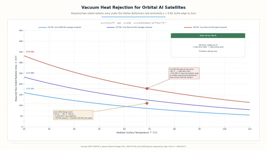
That incentive collides with the silicon. Leading-edge processors and HBM stacks prefer junction temperatures well below 100°C, and every degree of temperature drop between the die and the radiator surface, through cold plates, pumped fluid and the panel itself, must be subtracted from the temperature at which the radiator can operate. Radiator area is thus set by a chain of small temperature differences.
The real energy balance is more demanding than the ideal formula. A radiator in low Earth orbit does not see only cold space. It also sees the Earth, which emits on average about 240 watts per square metre of thermal infrared, and sunlight reflected from clouds.[50] Mounting the panels edge-on to the Sun, as the June design proposed, keeps direct sunlight off them, but Earth infrared and albedo still fall on the faces and must be subtracted from what they can reject. Coatings also degrade under ultraviolet light and atomic oxygen.
NASA’s surveys of spacecraft thermal control describe the hardware involved, from deployable radiators and loop heat pipes to pumped fluid loops, and every element has mass.[48] The International Space Station, the largest radiator system yet flown, rejects up to about 70 kilowatts of heat through large deployable panels cooled by pumped ammonia. SpaceX’s claim of an order-of-magnitude reduction in cooling power overhead can be true, since radiation needs no compressors or towers, while radiator mass remains a first-order term in the launch bill.[3] The official figure of 75 kilowatts per tonne is one way the company has chosen to express that trade.
13. Wings for a sunlit orbit
If radiators set the cooling budget of an orbital data centre, solar arrays set its power budget, and the two together define the silhouette of AI1. The satellite on the Starmind page is less a box than a pair of wings, spanning 75 metres, with a compute core between them.[3]
The June design assumed an array output of 250 watts per square metre.[47] Sunlight above the atmosphere at Earth’s distance delivers about 1,361 watts per square metre, the figure known as the solar constant, so 250 watts represents about 18 per cent end-to-end efficiency once cell efficiency, packing factor, temperature derating, wiring losses and power conversion are included.[50] That is within the range that NASA’s survey of small-spacecraft power systems would lead an engineer to expect from modern multi-junction or high-efficiency silicon arrays, and it is not a magic number.[51] At that output, a 250-kilowatt peak payload needs on the order of 1,000 square metres of array, before pumps, avionics and laser terminals.
The orbit is chosen to keep the arrays lit. In a dawn-dusk sun-synchronous orbit, the satellite rides above the line between day and night, its orbital plane precessing by about one degree a day so that it keeps the same orientation to the Sun throughout the year.[52] Such an orbit can avoid eclipse for most of the year, which is what the Starmind page means by “always sunny”.[3] It avoids the battery cycling of lower-inclination orbits, where shadow can occupy up to about a third of each orbit. The FCC application, however, also includes shells inclined at 30 degrees, and those satellites will pass through eclipse.[13]
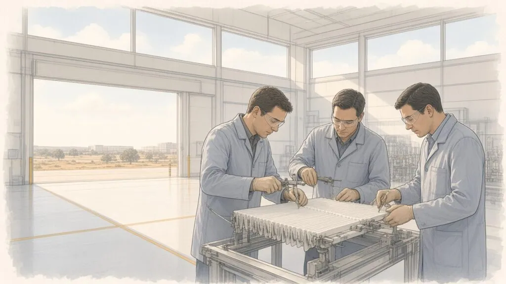
Building such wings is a problem of scale and precision on the ground. In an assembly hall, a deployable wing is tested by unfolding it across air-bearing tables or hanging it from gravity-offload rigs, so that hinges and tension cables can be exercised without being crushed by their own weight. Thermal engineers bond heat-pipe and fluid-loop panels and pressure-test the joints; metrology teams scan the surfaces with laser trackers, because a radiator that warps out of plane will see more of the Earth and less of space. Thermal-vacuum chambers then cycle complete assemblies through the temperature swings of orbit.
The Gigasat Factory in Bastrop is meant to do this at a rate no satellite builder has attempted for vehicles of this size. SpaceX says it is building the plant “to manufacture AI satellites at massive scale”, with thousands starting as soon as late 2027.[3] Starlink has shown that a satellite line can run at thousands of units a year, but AI1 is far larger, and its compute modules must be integrated with fluid loops whose failure would end the mission.
The laser links that carry results home are a further subsystem with its own pointing demands. Optical terminals must hold a beam on a distant partner while the wings flex. NASA’s survey of small-spacecraft communications records how quickly optical links have matured, and Starlink’s mesh is the most extensive yet built.[13]
The design lifetime of AI1 has not been published on the Starmind page. Commentators often assume about five years, roughly the life of a low-orbit communications satellite, but no official figure was found for this essay. It sets how often wings, radiators and chips must be replaced, and how much radiation the silicon must survive.
14. Leading-edge silicon in a radiation field
Low Earth orbit is not a benign environment for electronics. A satellite there passes through a flux of protons and electrons trapped in Earth’s magnetic field, is exposed to the energetic particles that the Sun releases during solar radiation storms, and is struck continually by galactic cosmic rays, nuclei accelerated to enormous energies elsewhere in the galaxy.[53] Near-polar sun-synchronous orbits also cross high latitudes, where the magnetic field shields less, and the South Atlantic Anomaly, where the inner belt dips close to Earth.
The effects on chips fall into a few well-defined categories, as catalogued by NASA’s Radiation Effects and Analysis group and its electronic-parts programme.[54][55] A single-event upset is a bit flipped by a passing charged particle, a soft error that can be corrected if it is detected. A single-event latch-up is a parasitic short circuit triggered by a particle strike, potentially destructive unless the power is cut quickly. Total ionising dose is the slow accumulation of charge in insulating layers, shifting transistor thresholds and raising leakage over the mission. Displacement damage degrades solar cells and some sensors.
Static memory is the classic canary for the first of these effects. An SRAM cell stores its bit as a small charge balanced between two inverters, and as cells shrink, the charge a particle must deposit to flip one falls. That makes the first Austin test vehicle, an SRAM array, a natural early instrument for measuring a new process’s sensitivity, as well as its yield.[27] Test campaigns expose such chips to beams of protons or heavy ions and count the upsets per bit.
Leading-edge gate-all-around and backside-power nodes are not inherently radiation-hardened. Smaller transistors hold less charge, which raises upset sensitivity, although their smaller volumes can reduce the chance of being struck at all, and thinner oxides tend to tolerate total dose better than older, thicker ones. How 14A-class RibbonFETs with PowerDirect behave under heavy-ion and proton beams is a question for measurement rather than inference, and no public data on it were found for this essay.[41] The new backside power network adds a further, untested surface.
The established mitigations are well understood, and none is free. Error-correcting codes on memory, including the chip-kill schemes used in servers, correct single upsets at the cost of extra bits and logic. Triple modular redundancy duplicates control circuits three times and votes on the result. Memory scrubbing rereads and corrects stored data before errors accumulate. Radiation-hardened-by-design cell libraries and spot shielding of aluminium or polyethylene reduce sensitivity, but cost area, power or mass. A space-optimised chip in the prospectus’s sense is therefore likely to be a mix of architectural redundancy and error correction rather than a special process flag.[19]
Artificial intelligence workloads offer some forgiveness. A neural network performing inference can often tolerate an occasional flipped bit in its activations with little effect on output, whereas a flipped bit in control logic or in a pointer can crash a system. Designers of space AI hardware can therefore protect control paths and weights heavily while leaving some datapaths lightly protected.
The radiation environment also shapes the economics. A chip that degrades over five years must be replaced by a launch, and a chip that survives longer reduces the replacement rate. The FCC filing contemplates different hardware versions across its orbital shells, which would allow the companies to learn from early satellites before committing later ones.[13] The interaction of process node, shielding mass and design life is one of the least visible trades in the programme.
15. The arithmetic of launch
The case for orbital compute is, in the end, a comparison of costs per watt delivered over a lifetime, and the largest cost in orbit is getting there. At the March event Musk tied the terawatt goal to a launch rate of “about 10 million tons to orbit per year” at “100 kilowatts per ton”.[16] The identity is exact. Ten million tonnes multiplied by one hundred kilowatts per tonne is one terawatt. What it requires depends on each term.
The first term is specific power, the compute delivered per tonne of satellite. The Starmind page quotes 75 kilowatts per tonne, not 100.[3] At that figure, a terawatt a year would need about 13.3 million tonnes in orbit annually, a third more than the March number, unless efficiency is defined differently, for example as peak rather than average power. The gap between 175 kilowatts average and 250 peak on the same vehicle is itself a factor of 1.43.
The second term is launch rate. The entire mass launched to orbit in the history of spaceflight is far below ten million tonnes. The vehicle meant to change this is Starship, which the prospectus describes as “designed to be the world’s first fully and rapidly reusable spacecraft”, with which SpaceX aims “to reduce the cost to reach orbit by 99% or more relative to the historical average launch cost”.[19] Musk has said in other 2026 remarks that he believes Starship can reach less than $100 per kilogram, a target rather than a published price, and one that the prospectus does not state numerically.
A simple calculation shows why that target matters. At $100 per kilogram, launching one tonne of satellite costs $100,000. At 75 kilowatts per tonne, that is about $1.33 per watt of compute capacity for launch alone, before the cost of building the satellite. At $1,000 per kilogram, the figure rises to about $13 per watt. Orbital economics therefore turn on launch cost and specific power more than on chips.
The comparison on the ground is not with a free alternative. A terrestrial data centre pays for land, power and cooling, and often waits years for a grid connection. The International Energy Agency’s analysis of energy and AI shows data-centre electricity demand rising quickly and unevenly, concentrated where grids are already strained. The Terafab website concludes that space is “the only truly scalable solution for the future of AI”, a conclusion that depends on launch costs not yet demonstrated.[5]
Scale introduces a third term, the orbital environment. A million satellites would be many times more than all the active satellites in orbit in 2026, and the European Space Agency’s space-debris office and NASA’s Orbital Debris Program Office track a population of debris that already requires routine collision avoidance.[56] Large wings and radiators present large cross-sections to micrometeoroids and small debris, and the fluid loops behind them are vulnerable to punctures. Shells up to 2,000 kilometres high would also place satellites where atmospheric drag no longer clears failed hardware within a few years.[13]
None of this makes the arithmetic wrong; it makes it conditional. SpaceX’s prospectus treats deployment from 2028 as an expectation subject to “significant technical complexity, capital requirements, new innovations and regulatory approvals”.[19] The ten-million-tonne figure is best read as a measure of how much must change, not as a forecast of what will.
16. Power, water and policy on the ground
Whatever happens in orbit, Terafab itself will be a terrestrial factory with terrestrial needs, and the largest of them is electricity. Musk wrote on 22 March that the full plant would need “over 10GW of power at full scale”.[18] Ten gigawatts drawn continuously for a year amounts to about 87.6 terawatt-hours, roughly 2 per cent of all the electricity consumed in the United States and comparable to the output of several large nuclear stations.[57] Texas, which leads the country in electricity production and runs its own grid through ERCOT, is the obvious host, but even there such a load would be among the largest ever proposed.
The filings indicate how the companies intend to meet it. The JETI applications list on-site power generation, backup generation, substations and utility-scale battery storage among the eligible property.[30] On 30 August Musk wrote that “power quality can be solved with Tesla Megapacks” and that “there isn’t enough nearby land to power Terafab entirely with solar, but it will be partially solar-powered”.[58] The picture is of a behind-the-meter industrial power plant rather than a retail grid customer.
That choice has consequences beyond engineering. On-site thermal generation requires fuel supply, which in Texas would most likely mean natural gas, and air permits from the Texas Commission on Environmental Quality, whose air permitting programme governs new combustion sources.[59] The applications list these facilities but do not size them, and no official megawatt or emissions figures for the Grimes campus were found for this essay.[30] Fabs also need clean power, since a brief voltage sag can scrap wafers in process, the role Musk assigns to batteries.[58]
Water is the second need. A leading-edge fab uses ultrapure water, purified to parts-per-trillion impurity levels, to rinse wafers between process steps, and peer projects in Arizona, Ohio and Texas are typically described in terms of millions of gallons a day, much of it recycled. The Phase 1 text lists water treatment and recycling and industrial waste treatment, but not volumes.[30] Dry cooler arrays in the same list suggest an effort to limit evaporative losses.[30]
Policy is the third. Terafab sits inside a decade of industrial policy that began with the federal CHIPS and Science Act of 2022, administered through the Commerce Department and its National Institute of Standards and Technology. The awards documented by the Congressional Research Service went to established chipmakers such as Intel, TSMC, Samsung and Micron.[35] No primary source found for this essay shows a federal CHIPS award to TeraFab AI, LLC, Tesla or SpaceX for the Grimes campus, and none should be assumed. The incentives in play are state and local, JETI, the county agreements and a reported Texas Enterprise Fund grant.[2][33]
Geopolitics runs beneath the whole project. Musk’s January remark about protection “against any geopolitical risks” and the JETI applications’ language of a domestically controlled semiconductor ecosystem both point to the concentration of leading-edge logic in Taiwan and of memory in South Korea.[7][30] Micron’s US expansion in Idaho and New York is the main attempt to rebuild American memory production, on a slower clock than Terafab’s.
The equipment supply chain is international in any case. Lithography comes from ASML in the Netherlands, deposition and etch tools from companies such as Lam Research and Tokyo Electron, and inspection from KLA, with design software from firms such as Synopsys. The November reports of Terafab’s approaches to Japanese toolmakers are the first public sign of a purchasing campaign on the scale the filings imply.[44] A factory built to reduce dependence on foreign supply chains will, for its first decade at least, depend on them for the machines that make it work.
17. The clock and the claim
By the autumn of 2026 Terafab had acquired a timetable. On a SpaceX conference call around 20 October, Musk was reported as targeting volume production in the third quarter of 2028, with the fourth quarter also possible, and a first functional SRAM test chip in Austin in roughly May or June 2027.[27] He called the dates “very aggressive” and “insanely fast”.[27] Earlier that month he had settled a question of control, writing “No, we will build and run the fab. Let there be ZERO doubt about that.”[22]
The benchmark against which those dates should be judged is the industry’s own record. Leading-edge logic fabs built in the United States in the 2020s, tracked by the Semiconductor Industry Association, have typically taken three years or more from groundbreaking to volume production. The JETI impact tables themselves show no operating jobs at Grimes County until 2029, with construction concentrated in 2027 and 2028.[30] A volume start in the second half of 2028 would therefore be fast by any precedent, though not physically impossible for a single-product line with assured demand.
The pace of public statements has continued to rise. In October and November Musk used X to recruit engineers and to describe the project as moving quickly, at times in terms of output measured against national economies.[60][61] Such posts are signals of intent and of hiring, not schedule commitments, and they sit alongside a prospectus that, as of its filing, contained no development timeline at all.[19]
What, then, would success look like at each stage? In 2027 it would be functional SRAM and logic test structures from the Austin research fab, followed by evidence that its design-to-silicon loop is measured in days rather than months. In 2027 and 2028 it would be the first AI1 satellites in sun-synchronous orbit, initially on NVIDIA hardware, rejecting their heat through radiators whose performance can be compared with the June and November figures.[3][36] From 2028 it would be wafers moving at Gibbons Creek, a published water and power plan, and definitive agreements among Tesla, SpaceX and Intel.
Each of these milestones is observable. Musk’s estimate of an investment of “over a trillion dollars long-term”, conditional on a terawatt a year of silicon, cannot be tested for many years.[34] The $5 billion county minimum by 2030 and the 1,800 jobs by 2035 can be.[33] Between those numbers lies every outcome from a successful captive fab that never nears a terawatt to the transformation the website describes.
The physics does not settle the argument but frames it. A radiator in vacuum must reject every watt through \( \sigma T^4 \), and power density in orbit is bought with area and mass. A leading-edge transistor in a radiation field must be protected by redundancy that costs area and power. A 14A line must climb a yield curve that no amount of rhetoric can shorten. The launch arithmetic is exact; the uncertainty lies in cost per kilogram and kilowatts per tonne.
Terafab is, in the end, an attempt to make the physical layer of artificial intelligence as iterable as its software, and to place much of that layer above the atmosphere. Its own legal documents describe it as a framework whose specific projects “have not yet been determined”.[19] Its filings in Texas describe phases that may or may not be built, and its satellites are still being redesigned. The most accurate account of the project in November 2026 is that of a very large stated ambition, with a documented, very aggressive clock, in which every major figure is a commitment of a different kind.
18. Timeline
Nikolai Kardashev classifies civilisations by the energy they command, a frame later borrowed by Terafab.
Texas awards SpaceX a $17.3 million semiconductor grant for Bastrop, an instrument separate from Terafab.
Musk assigns roles to AI5, AI6 and AI7 or Dojo3 and restarts Dojo3 for space computing.
On Tesla’s fourth-quarter call Musk says the company must build “a Tesla Terafab” for logic, memory and packaging.
A SpaceX affiliate asks the FCC to authorise up to one million orbital data-centre satellites.
Tesla and SpaceX launch Terafab in Austin with a goal of a terawatt of compute a year, about 80 per cent for space.
Intel announces that it will join the project as a process and packaging partner.
Tesla breaks ground on the research fab at Giga Texas and completes the final design of AI5.
Musk names Intel’s 14A as the planned process and describes a research fab of about $3 billion.
SpaceX gives notice of a Gibbons Creek campus costing $55 billion for initial phases and $119 billion if expanded.
The S-1 and final prospectus define Terafab while stating that its specific projects have not yet been determined.
Grimes County approves a reinvestment zone, a tax abatement and an economic development agreement.
TeraFab AI, LLC files eight school-district applications covering four phases, with $16.801 billion eligible in Phase 1.
A SpaceX video describes AI1 at about 150 kW peak and 120 kW average with a 70-metre wingspan.
Tesla confirms the Grimes County site, and Musk estimates about 75 per cent of output for AI spacecraft.
JETI agreements are posted, and NVIDIA says the first Starmind satellite will use an optimised Vera Rubin NVL72.
Tesla, SpaceX and SpaceXAI ask a federal court in Austin to rule on the Terafab name.
Musk says the companies will build and run the fab and targets volume production in late 2028.
Korean reporting says Terafab has sought about one million wafers a month after 2032, a figure absent from company filings.
Targets call for an SRAM test chip in Austin by mid-year and Gigasat production from as soon as late 2027.
Volume production is targeted for the second half, and orbital deployment as early as this year.
The county agreement requires $5 billion of investment by 2030 and 1,800 jobs by 2035, and the fourth JETI phase runs to 2036.
References
- Tesla on X, “Terafab will be built in Grimes County, Texas”, 6 August 2026 *
- Texas Comptroller of Public Accounts, “JETI Current Agreements” *
- SpaceX, “Starmind” *
- U.S. Securities and Exchange Commission, “Space Exploration Technologies Corp., Form S-1 Registration Statement”, 20 May 2026 *
- Terafab, “TERAFAB”, official project site *
- Elon Musk on X, “Formal announcement of the TERAFAB project”, 21 March 2026 *
- StockAnalysis, “Tesla Q4 2025 Earnings Call Transcript”, 28 January 2026 *
- Elon Musk on X, “Terafab will technically be two fabs”, 22 March 2026 *
- Elon Musk on X, post on the AI5 and AI6 design cycle, 17 January 2026 *
- Elon Musk on X, post on the AI4 to AI7 roadmap, 18 January 2026 *
- Elon Musk on X, post on restarting Dojo3, 18 January 2026 *
- Elon Musk on X, post on chips for space at gigawatt scale, 1 February 2026 *
- Federal Communications Commission, Space Bureau, “Public Notice DA 26-113, SpaceX Orbital Data Center System”, 4 February 2026 *
- SpaceX on X, “Announcing TERAFAB”, 22 March 2026 *
- Elon Musk on X, “SpaceXAI + Tesla TERAFAB Project”, 22 March 2026 *
- YouTube, “TERAFAB, The Largest Chip Manufacturing Facility Ever”, recording of the 21 March 2026 launch *
- SpaceX on X, post on Starmind and Terafab as a step toward Kardashev Type II, 16 July 2026 *
- Elon Musk on X, post on the Austin advanced technology fab and the full-scale site, 22 March 2026 *
- U.S. Securities and Exchange Commission, “Space Exploration Technologies Corp., Form 424B4 Prospectus”, 12 June 2026 *
- Intel on X, “Intel is proud to join the Terafab project”, 7 April 2026 *
- Elon Musk on X, “Looking forward to working with Intel on the Terafab”, 7 April 2026 *
- Elon Musk on X, “We will build and run the fab”, 7 October 2026 *
- TERA-print, “Litigation” *
- U.S. District Court, Western District of Texas, “Tesla, Inc. v. TERA-print, LLC, Complaint”, 15 September 2026 *
- CourtListener, “Tesla, Inc. v. TERA-print, LLC, 1:26-cv-02543” *
- StockAnalysis, “Tesla Q1 2026 Earnings Call Transcript”, 22 April 2026 *
- TrendForce, “Musk Targets Terafab Chip Volume Production in 3Q28, First SRAM Test Chip by Mid-2027”, 21 October 2026 *
- Tesla, “Q1 2026 Update”, 22 April 2026 *
- CNBC, “Elon Musk’s SpaceX chip fab in Texas to cost up to $119 billion”, 6 May 2026 *
- Texas Comptroller of Public Accounts, “JETI Application J0035, TeraFab AI, LLC, Anderson-Shiro CISD” *
- Texas Comptroller of Public Accounts, “JETI Application J0039, TeraFab AI, LLC, Iola ISD” *
- Grimes County Citizens for Responsible Development, “Combined Summary, Iola and Anderson-Shiro ISD JETI Applications” *
- KBTX, “Grimes County officially releases SpaceX Terafab agreement documents”, 6 June 2026 *
- Elon Musk on X, “Terafab will be over a trillion dollars long-term”, 29 August 2026 *
- Congressional Research Service, “Semiconductor Fabrication Facilities Funded by the CHIPS Act”, R49031 *
- NVIDIA Newsroom, “SpaceXAI Adopts NVIDIA Vera CPU to Accelerate Agentic AI at Massive Scale”, 24 August 2026 *
- Elon Musk on X, post on the Optimus and AI spacecraft split, 6 August 2026 *
- Engineering News-Record, “SpaceX Records Fight Exposes $119B Terafab Buildout Plans” *
- Elon Musk on X, “This will be a very capable chip”, 19 January 2026 *
- NVIDIA Newsroom, “NVIDIA Launches Space Computing”, 16 March 2026 *
- Intel Foundry, “Process Technology” *
- ASML, “TWINSCAN EXE:5000” *
- Intel Newsroom, “Intel Foundry and ASML Accelerate Industry Readiness for High-NA EUV”, 7 September 2026 *
- Financial News, report on Terafab wafer procurement, 9 November 2026 *
- TrendForce, “Terafab Reportedly Eyes 1M Wafers Monthly by 2032, with 700K for Memory”, 9 November 2026 *
- Tom’s Hardware, “Elon Musk’s Terafab targets 1 million wafers a month after 2032”, November 2026 *
- Data Center Dynamics, “SpaceX details AI1 satellite data center, claims 150kW peak compute”, 9 June 2026 *
- NASA Small Spacecraft Systems Virtual Institute, “Thermal Control” *
- NIST, CODATA Fundamental Physical Constants, “Stefan - Boltzmann constant” *
- NASA Earth Observatory, “Climate and Earth’s Energy Budget” *
- NASA Small Spacecraft Systems Virtual Institute, “Power” *
- European Space Agency, “Types of orbits” *
- NOAA Space Weather Prediction Center, “Solar Radiation Storm” *
- NASA Goddard Space Flight Center, “Radiation Effects and Analysis” *
- NASA Electronic Parts and Packaging Program *
- European Space Agency, “Space Debris” *
- U.S. Energy Information Administration, “Use of electricity” *
- Elon Musk on X, “Power quality can be solved with Tesla Megapacks”, 30 August 2026 *
- Texas Commission on Environmental Quality, “Air Permits” *
- Elon Musk on X, “Join the Terafab project”, 12 October 2026 *
- Elon Musk on X, “Terafab is moving fast”, 6 November 2026 *