How a Chip Is Made
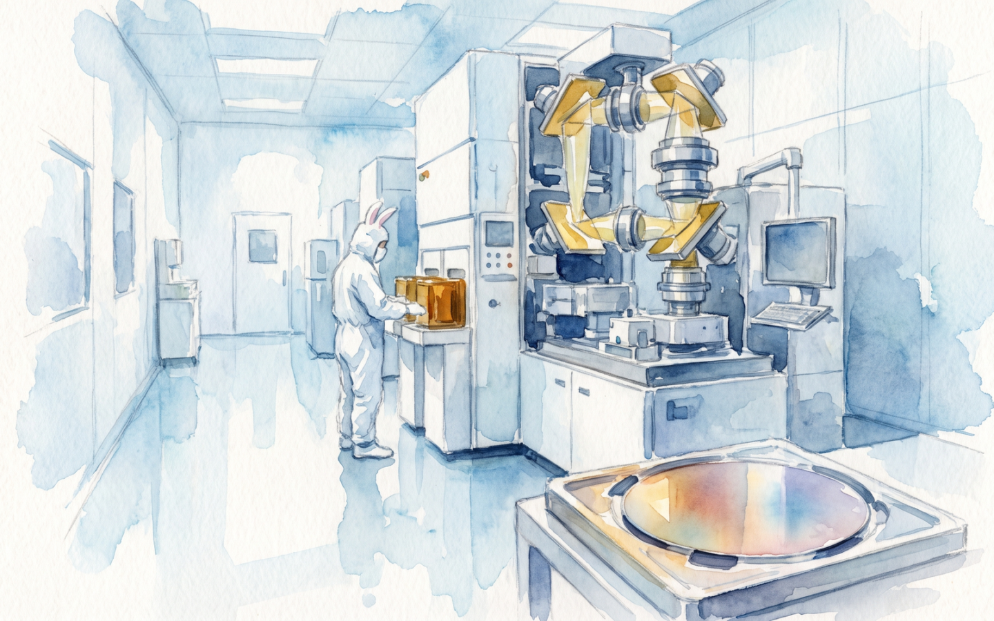
A modern smartphone contains a chip with more than twenty billion transistors, the smallest features only a few nanometres across, fabricated in a factory that cost more than twenty billion dollars to build. The story of how a chip is made is a story of light, chemistry, vacuum, and an astonishingly global supply chain. It is also a story of how a single company in the Netherlands came to own the machine that draws the smallest features, and how a single company in Taiwan came to own the factory that uses it. This post is an attempt to explain, in roughly four thousand words, what actually happens inside a leading-edge semiconductor fab, from a polished silicon wafer to a packaged, tested, working chip.
Key findings
- The clean room is the heart of the fab, and it is more important than the equipment. A modern leading-edge fab operates in a class 1 clean room, with fewer than ten particles larger than 0.5 micrometres per cubic metre of air. The reason is that a single dust particle landing on a mask or a wafer can kill a chip. The clean room, the bunny suits, the air showers, the wafer-handling robots, the FOUPs (front-opening unified pods), and the SMIF (standard mechanical interface) systems are the unglamorous infrastructure that makes the rest possible.[1, 2, 3]
- Photolithography is the workhorse — drawing circuits with light through a mask. The fundamental process has not changed since the 1960s: a silicon wafer is coated with a light-sensitive photoresist, the photoresist is exposed to ultraviolet light through a patterned mask (or reticle), the exposed photoresist is dissolved in a developer, and the underlying material is etched away in the gaps. The patterning step is then repeated, often forty or fifty times, with different masks, different etches, and different depositions, to build up the three-dimensional structure of a transistor and its wiring.[4, 5, 6]
- EUV lithography at 13.5 nm wavelength is the technology that broke the resolution barrier. For two decades, the industry shrank transistor dimensions by using shorter and shorter wavelengths of ultraviolet light. By the early 2010s, the wavelength of the light used in mass production (193 nm, deep ultraviolet) was larger than the smallest features being drawn. The only practical way to keep shrinking was to switch to extreme ultraviolet (EUV) lithography, at 13.5 nm wavelength. EUV was the most ambitious manufacturing technology project of the early twenty-first century. It is now the technology that every leading-edge chip depends on, and the only company in the world that makes production EUV scanners is ASML, based in Veldhoven in the Netherlands.[7, 8, 9]
- Transistors are made by repeatedly depositing, patterning, etching, and doping. The process flow for a modern FinFET or gate-all-around transistor takes four to six months from bare wafer to finished die, and involves hundreds of individual steps. The four basic operations are oxidation (growing silicon dioxide), deposition (putting down layers of silicon, silicon nitride, metals, or dielectrics), lithography (patterning), and etch (removing material in the patterned gaps). Dopants are introduced by ion implantation or by diffusion, and the whole structure is built up in dozens of metal layers, connected by tiny copper vias.[4, 10, 11]
- Yield and metrology make the difference between a fab that makes money and one that does not. A leading-edge wafer may contain several hundred individual chips, each with tens of billions of transistors. A single defect anywhere in the process can kill one chip; a systematic problem can kill the whole wafer. The metrology (inspection and measurement) tools that catch defects are themselves multi-million-dollar instruments, and the statistical process control that runs the fab is one of the most complex real-time control systems in industry. A new fab typically takes two to three years to reach commercially usable yield, and a one-percent yield improvement on a leading-edge process is worth more than a billion dollars a year.[12, 13, 14]
- A modern leading-edge fab costs more than twenty billion dollars and depends on a global supply chain of perhaps one thousand companies. The TSMC fab in Hsinchu, Taiwan, that makes 3-nm chips cost an estimated twenty billion dollars; the company’s planned fab in Arizona is expected to cost a similar amount. Inside each fab are stepper and EUV scanners from ASML, etch tools from Lam Research and Tokyo Electron, deposition tools from Applied Materials, inspection tools from KLA, and photoresists from a small number of Japanese and American chemical companies. The supply chain is, by some estimates, the most complex in industrial history.[15, 16, 17]
The clean room and the wafer
The starting point of a modern chip is a circular disc of pure silicon, three hundred millimetres in diameter and less than a millimetre thick, polished to a surface roughness of less than half a nanometre. The silicon has been grown as a single crystal by the Czochralski process, doped with boron or phosphorus to give it the right electrical properties, and sliced from a 300 mm ingot with a wire saw. A single ingot can weigh more than a hundred kilograms and produce several hundred wafers. The purity of the silicon is extraordinary: more than 99.9999999 percent pure (nine nines), with controlled impurity concentrations in the parts-per-trillion range.[1, 2, 18]
The wafers are loaded into plastic cassettes called FOUPs (front-opening unified pods) and brought into the clean room. The clean room itself is the first piece of technology that anyone visiting a fab notices. The air is filtered continuously through HEPA and ULPA filters, removing particles down to a few nanometres in size. The room is pressurised slightly above atmospheric, so that any leak flows outward, not inward. The temperature and humidity are tightly controlled. The workers wear full-body bunny suits, hoods, gloves, boots, and masks, and pass through air showers before entering. The reason is simple: a single 50-nm dust particle landing on a wafer during a critical lithography step can disrupt the patterning of an entire chip, and a single disrupted chip is a dead chip.[2, 3, 19]
Inside the clean room, the wafers are moved by automated tracks and robotic handlers, not by people. The lithography, etch, deposition, and inspection tools are connected to a central material-handling system that moves FOUPs between them without ever exposing a wafer to the open air. A single FOUP might travel through forty or fifty different tools over the four to six months of its process flow, accumulating perhaps five hundred individual steps. The total distance it travels inside the fab, in a modern 300 mm line, is measured in kilometres.[3, 20]
Photolithography: drawing circuits with light
The single most important step in chip manufacturing is photolithography. The basic idea has not changed in sixty years. A silicon wafer is coated with a thin layer of photoresist, a light-sensitive polymer. The wafer is then exposed to ultraviolet light through a mask (or reticle), a glass plate with the pattern of one layer of the circuit drawn on it as an opaque layer of chrome. Where the light passes through the clear parts of the mask, it changes the chemistry of the photoresist; where it is blocked by the chrome, the photoresist is unchanged. The wafer is then immersed in a developer, which dissolves away the exposed (positive-tone) photoresist, leaving a patterned stencil on the wafer. The stencil is used to control the next step — typically an etch or an ion implant — and the photoresist is then stripped away.[4, 5, 21]
The resolution of the patterning — the smallest feature that can be drawn — is set by the wavelength of the light used, the numerical aperture of the lens, and the refractive index of the medium between the lens and the wafer. The classical formula, the Rayleigh criterion, says that the minimum feature size is proportional to the wavelength, and inversely proportional to the numerical aperture. To draw smaller features, the industry had to use shorter and shorter wavelengths.[5, 6]
The progression in the late twentieth century was from mercury g-line (436 nm) to i-line (365 nm) to deep ultraviolet (DUV) at 248 nm (using a krypton fluoride excimer laser) and then 193 nm (using an argon fluoride excimer laser). By the early 2010s, the 193 nm wavelength had been pushed well past its theoretical diffraction limit, using tricks such as immersion lithography (a film of water between the final lens and the wafer, increasing the numerical aperture beyond 1.0), phase-shift masks, optical proximity correction, and double- or quadruple-patterning (in which a single layer is exposed two or four times with different masks, multiplying the effective resolution). The result was that the industry could, with great difficulty, draw features down to about 20 nm using 193 nm light. The cost was enormous: every additional patterning step adds weeks of process time and tens of millions of dollars in mask and tool cost.[6, 7, 22]
To go smaller, the industry needed shorter-wavelength light. The natural choice was extreme ultraviolet (EUV), at a wavelength of 13.5 nm. But 13.5 nm light is absorbed by every known solid material and by every known gas. It can only be transmitted in a vacuum. The optics cannot be lenses — they have to be mirrors, made of multilayer Bragg reflectors alternating molybdenum and silicon, with a reflectivity of about 70 percent per surface (so a system of ten mirrors has a transmission of less than three percent). The light source itself has to be a tin plasma, heated by a high-power carbon dioxide laser to a temperature of about 200,000 degrees, emitting 13.5 nm photons in every direction; only a small fraction of those photons end up at the wafer. The whole system is the most complex light source ever built for industrial use, and the engineering effort to make it work took three decades and cost more than ten billion dollars.[7, 8, 23]
EUV and the 13.5 nm problem
The transition to EUV was the single most ambitious manufacturing technology project of the early twenty-first century. The technical challenges were formidable. The light source, developed by ASML in partnership with Trumpf and Siemens, works by firing a tin droplet 25 micrometres across at high speed into a vacuum chamber, hitting it with a high-power pre-pulse laser to flatten it into a pancake, and then hitting it with the main CO2 laser pulse. The tin plasma reaches a temperature of about 200,000 kelvin, hotter than the surface of the sun, and emits EUV photons. A modern ASML EUV scanner has two tin droplet generators, fires 50,000 droplets per second, and produces about 250 watts of EUV power at the intermediate focus. A next-generation scanner, already in customer trials, produces 500 W, and the long-term target is 1,000 W.[7, 8, 24]
The mirrors are made by Zeiss in Germany, with surface figures accurate to a few atoms, polished for months and coated with about fifty alternating layers of molybdenum and silicon. The mask is also reflective — a glass substrate with a multilayer Mo/Si Bragg reflector and an absorber pattern on top. The mask blank itself is one of the most perfect surfaces ever manufactured, with a flatness of about 0.15 nm across a 150 mm square. The pellicle that protects the mask from particles is a 50-nm-thick free-standing film of polysilicon, transparent to EUV and able to survive the scanner’s vacuum environment for years.[8, 23, 25]
ASML is now the sole supplier of EUV scanners in the world. The company, founded in 1984 as a joint venture between Philips and ASM International, makes both EUV and DUV scanners, plus the metrology and inspection tools that go with them. The most advanced current model, the TWINSCAN NXE:3800E, costs about $200 million per unit, weighs about 150 tonnes, and takes about a year to install. ASML’s 2024 revenue was about 28 billion euros, and the company has an order backlog stretching several years into the future. The only credible competitor, the Japanese firm Nikon, exited the EUV development race in the early 2000s. Canon is pursuing a competing technology, nanoimprint lithography, but it has not yet been adopted for high-volume manufacturing.[7, 9, 26]
The first commercial EUV chips were made by TSMC and Samsung in 2018–2019, at the 7 nm node. By 2024, EUV was used for the most critical layers of every leading-edge chip, at the 3 nm node and 2 nm node. The industry is now investing in high-numerical-aperture EUV (NA-EUV), with a numerical aperture of 0.55 instead of 0.33, which can resolve features down to about 8 nm in a single exposure. The first NA-EUV scanner, ASML’s TWINSCAN EXE:5000, was delivered to Intel in late 2023. The 0.55 NA system costs more than $350 million per unit, and Intel, TSMC, and Samsung have all ordered them.[9, 27, 28]
Etching, deposition, and the transistor
The transistor is the active element of every chip. A modern leading-edge transistor is a three-dimensional structure, only a few tens of nanometres across, made of silicon, silicon-germanium, silicon dioxide, silicon nitride, tungsten, cobalt, ruthenium, and copper. The classical planar transistor — a flat gate on top of a flat channel — was replaced in 2011 by the FinFET, in which the channel is a vertical fin of silicon rising from the substrate, with the gate wrapping around the fin on three sides. In 2022–2024, the industry began the transition to the gate-all-around (GAA) transistor, in which the channel is a stack of horizontal silicon nanosheets, with the gate wrapping around each sheet on all four sides. The GAA structure gives better electrostatic control, lower leakage, and higher drive current at a given footprint, but it is much harder to fabricate.[4, 10, 29]
The transistor is built up by repeating four basic operations: oxidation, deposition, lithography, and etch. Oxidation grows a thin layer of silicon dioxide on the silicon surface, by heating the wafer to about 1000°C in an oxygen-containing atmosphere. Deposition puts down a thin film of some material — silicon, silicon nitride, tungsten, copper, or a low-k dielectric — by chemical vapour deposition (CVD), physical vapour deposition (PVD), or atomic layer deposition (ALD). Lithography patterns the deposited film. Etch removes the parts of the film not protected by the photoresist, by exposing the wafer to a reactive plasma (typically a fluorine- or chlorine-containing gas in a low-pressure chamber with radio-frequency excitation). The four operations are then repeated with different materials and different masks, to build up the gate, the source and drain, the contacts, and the local interconnect.[4, 11, 30]
The metal wiring above the transistors is built up in successive layers, with each layer made by a damascene process. A layer of insulating low-k dielectric is deposited, patterned by lithography and etch to form trenches and vias, filled with copper by electrochemical deposition, and then polished back by chemical-mechanical polishing (CMP) to leave a flat surface. A modern chip has fifteen or more such metal layers, with the smallest at the bottom (near the transistors) and the largest at the top (for power distribution and global signalling). The smallest vias are now less than 10 nm in diameter; the largest wires at the top of the chip are several micrometres across.[10, 11]
After the last metal layer is finished, the wafer is passivated (covered with a protective layer of silicon nitride and polyimide), tested electrically with a wafer-level prober, and then diced into individual chips with a diamond saw. Each chip is then packaged — mounted on a lead frame or substrate, connected to the package by gold or copper bond wires or by flip-chip solder bumps, and encapsulated in plastic or ceramic. The packaged chip is then tested again, this time at full speed and over the full operating temperature range, and the bad ones are marked and discarded. The yield — the fraction of chips on a wafer that pass all tests — for a leading-edge process is typically 60–80 percent when the process is mature, and much lower when it is new.[12, 13]
Yield, metrology, and the economics of billions
The most important number in chip manufacturing is yield. A modern 300 mm wafer, at the 3 nm node, contains perhaps three hundred individual chips, each with twenty billion transistors and a market value of perhaps a thousand dollars. A single defect anywhere in the process can kill one of those chips, and a single defect on a mask can kill a hundred chips on every wafer. The metrology tools that catch defects before they become yield problems are themselves multi-million-dollar instruments: scanning electron microscopes that can resolve single atoms, optical inspection tools that can detect particles as small as 10 nm, and electrical testers that can probe the characteristics of individual transistors on a finished wafer.[12, 14]
The fab runs a statistical process control (SPC) system that monitors every tool and every wafer in real time, looking for drifts and excursions. When a tool drifts out of its control limits, it is taken offline for maintenance. When a wafer is found to be defective, it is reworked (if possible), sent to a scrap bin, or sent to engineering analysis. The data from the SPC system, accumulated over the years, is one of the most valuable assets a fab has; a new fab starting up with no historical data can take two to three years to reach commercially usable yield, and a one-percent yield improvement on a leading-edge process is worth more than a billion dollars a year in additional revenue.[12, 14, 31]
The cost of a modern leading-edge fab is now more than twenty billion dollars. The TSMC fab in Hsinchu, Taiwan, that makes 3 nm chips cost an estimated twenty billion dollars; the company’s planned Arizona fab is expected to cost a similar amount. The fab building itself, with its clean room, its ultrapure water systems, its chemical delivery systems, and its gas plants, accounts for perhaps a quarter of the cost. The lithography tools account for another quarter (one EUV scanner is $200 million, and a fab needs twenty or thirty of them). The etch, deposition, and inspection tools account for another quarter. The remaining quarter is everything else — from the wafer-handling robots to the IT infrastructure.[15, 16, 32]
Geopolitics: the foundry race
The concentration of leading-edge chip manufacturing in Taiwan — and to a lesser extent South Korea — is one of the most discussed strategic vulnerabilities in the global economy. As of 2024, TSMC manufactured more than 90 percent of the world’s most advanced logic chips, those at the 7 nm node and below. Samsung in South Korea accounts for most of the rest. The United States, Europe, and Japan, despite designing the majority of the world’s leading-edge chips, manufacture almost none of them at the leading edge. The chip shortage of 2020–2022, caused by the Covid-19 pandemic and its aftermath, brought this concentration into sharp focus.[16, 17, 33]
The response, in the United States, was the CHIPS and Science Act of 2022, which allocated 52 billion dollars in subsidies and tax credits for domestic chip manufacturing. The response in Europe was the European Chips Act of 2023, which committed 43 billion euros to a similar end. The response in Japan was a combination of subsidies and industrial policy, focused on bringing TSMC and Samsung fabs to Kumamoto and elsewhere. The response in China was a massive state-led investment in domestic fabs, combined with efforts to develop domestic alternatives to EUV lithography, which the United States has so far blocked from sale to China.[17, 33, 34]
The new fabs coming online in Arizona, Texas, Ohio, Germany, Japan, and elsewhere over the next five years will diversify the geographic concentration, but they will not break the foundry model. The economics of the leading edge — the twenty-billion-dollar fab, the two-to-three-year yield ramp, the dependence on ASML, on Zeiss, on a small number of chemical suppliers — favour the companies and the regions that have been doing it for decades. TSMC, Samsung, and (with a large public investment) Intel are likely to remain the only three companies in the world that can build leading-edge logic chips for the foreseeable future. The rest of the industry — the designers, the equipment makers, the materials suppliers, the EDA software houses, the IP licensors — is global, but the manufacturing is, for the moment, a three-company oligopoly centred on northeast Asia.[15, 16, 33]
What is in it for science
Semiconductor manufacturing is, in a real sense, the most demanding applied-science project in industrial history. The combination of physics (quantum mechanics, plasma physics, optics, materials science), chemistry (CVD precursors, photoresists, etchants, dopants), and engineering (vacuum systems, robotics, software, statistical process control) is broader than almost any other field. The cost of building a leading-edge fab is now comparable to the cost of a major new particle accelerator, and the number of people involved — perhaps a hundred thousand across the industry — is comparable to the number involved in a large astronomical observatory or a flagship oceanographic programme. The fact that this industry has continued to deliver, on something close to Moore’s-law cadence, for sixty years is, in retrospect, one of the great achievements of late-twentieth and early-twenty-first-century science. The fact that its future is now constrained by geopolitics, by the limits of physics, and by the cost of the next fab is, in equal measure, one of the great challenges.[35, 36, 37]
Comparison: leading-edge foundries (2024)
| Company | Headquarters | Most advanced node in production (2024) | Approx. capex 2024 (US$ bn) | Market share at 7 nm and below |
|---|---|---|---|---|
| TSMC | Hsinchu, Taiwan | 3 nm (N3), with 2 nm in risk production | ~30 | ~90 percent |
| Samsung Foundry | Suwon, South Korea | 3 nm (3GAP), with 2 nm in development | ~25 | ~8 percent |
| Intel Foundry | Santa Clara, California | Intel 4 (7 nm-class) in production, Intel 18A (1.8 nm-class) in development | ~25 | ~1 percent |
Key numbers
- $200 million: cost of one ASML EUV scanner (NXE:3800E).
- $350 million: cost of one ASML NA-EUV scanner (EXE:5000).
- 13.5 nm: wavelength of EUV light, smaller than the size of many viruses.
- 200,000 °C: temperature of the tin plasma that emits EUV light inside an ASML scanner.
- 50,000 per second: number of tin droplets fired by a modern EUV source.
- 250 W: usable EUV power at the intermediate focus of a modern production scanner.
- 150 tonnes: weight of a single ASML EUV scanner.
- ~20 billion: number of transistors in a 3 nm smartphone chip (e.g. Apple A18 Pro).
- 40–50: number of lithography steps in a 3 nm process flow.
- 15–18: number of metal interconnect layers in a 3 nm chip.
- 4–6 months: total time from bare wafer to finished die.
- 60–80 percent: typical yield of a mature leading-edge process.
- $20+ billion: cost of a new leading-edge fab.
References
- Wikipedia, “Semiconductor fabrication plant.” (Standard reference on fab structure and clean-room classification.) https://en.wikipedia.org/wiki/Semiconductor_fabrication_plant
- Wikipedia, “Cleanroom.” (Standard reference on clean-room standards and the Federal Standard 209E classification.) https://en.wikipedia.org/wiki/Cleanroom
- SEMI. Semiconductor Manufacturing: A Guide to Fab Operations. San Jose, CA: Semiconductor Equipment and Materials International, 2023. (The industry-standard reference on fab operations.)
- Plummer, J. D., M. D. Deal, and P. B. Griffin. Silicon VLSI Technology: Fundamentals, Practice and Modeling. Upper Saddle River, NJ: Prentice Hall, 2000. (The standard textbook on silicon VLSI process integration.)
- Wikipedia, “Photolithography.” (Standard reference on photolithography.) https://en.wikipedia.org/wiki/Photolithography
- Wikipedia, “Deep ultraviolet lithography.” (Standard reference on DUV lithography and immersion lithography.) https://en.wikipedia.org/wiki/Deep_ultraviolet_lithography
- Wikipedia, “Extreme ultraviolet lithography.” (Standard reference on EUV lithography, with sources on the technology history.) https://en.wikipedia.org/wiki/Extreme_ultraviolet_lithography
- ASML. “EUV lithography: technology explained.” Corporate technical brief, 2024. https://www.asml.com/en/technology/euv-lithography
- Wikipedia, “ASML.” (Standard reference on ASML, with revenue and market share data.) https://en.wikipedia.org/wiki/ASML
- Wikipedia, “FinFET.” (Standard reference on the FinFET transistor.) https://en.wikipedia.org/wiki/FinFET
- Wikipedia, “Multi-gate MOSFET.” (Standard reference on gate-all-around and multi-gate transistor architectures.) https://en.wikipedia.org/wiki/Multi-gate_MOSFET
- Wikipedia, “Semiconductor yield.” (Standard reference on yield modelling and defect-density calculations.) https://en.wikipedia.org/wiki/Semiconductor_yield
- Wikipedia, “Statistical process control.” (Standard reference on SPC in semiconductor manufacturing.) https://en.wikipedia.org/wiki/Statistical_process_control
- KLA Corporation. “Process control and yield management in advanced semiconductor manufacturing.” Corporate technical brief, 2024. https://www.kla.com/
- Khan, S. M., A. Mann, and D. Peterson. “The Semiconductor Supply Chain: Assessing National Competitiveness.” Center for Security and Emerging Technology, January 2021. (A leading independent analysis of the semiconductor supply chain.)
- Wikipedia, “TSMC.” (Standard reference on TSMC, with revenue and capacity data.) https://en.wikipedia.org/wiki/TSMC
- Wikipedia, “CHIPS and Science Act.” (Standard reference on the 2022 US CHIPS Act.) https://en.wikipedia.org/wiki/CHIPS_and_Science_Act
- Wikipedia, “Czochralski process.” (Standard reference on silicon crystal growth.) https://en.wikipedia.org/wiki/Czochralski_process
- Whyte, W. Cleanroom Technology: Fundamentals of Design, Testing and Operation. London: John Wiley & Sons, 2001. (The standard textbook on clean-room design and operation.)
- Burgess, J. Semiconductor Production: A Technician’s Guide. Berlin: Springer, 2022. (A modern textbook on semiconductor production.)
- Wikipedia, “Photoresist.” (Standard reference on photoresist chemistry.) https://en.wikipedia.org/wiki/Photoresist
- Wikipedia, “Immersion lithography.” (Standard reference on immersion lithography and numerical aperture.) https://en.wikipedia.org/wiki/Immersion_lithography
- Wikipedia, “Bragg reflector.” (Standard reference on multilayer Bragg reflectors used in EUV optics.) https://en.wikipedia.org/wiki/Bragg_reflector
- Wikipedia, “Carbon dioxide laser.” (Standard reference on the CO2 laser used in EUV sources.) https://en.wikipedia.org/wiki/Carbon_dioxide_laser
- Wikipedia, “Carl Zeiss (company).” (Standard reference on Zeiss and the EUV mirror program.) https://en.wikipedia.org/wiki/Carl_Zeiss
- Wikipedia, “Nikon.” (Standard reference on Nikon and the company’s history in lithography.) https://en.wikipedia.org/wiki/Nikon
- ASML. “High-NA EUV lithography: the next step.” Corporate technical brief, 2024. https://www.asml.com/en/technology/high-na-euv-lithography
- Intel Corporation. “Intel Foundry: process roadmap.” Corporate technical brief, 2024. https://www.intel.com/content/www/us/en/foundry.html
- Wikipedia, “Damascene process.” (Standard reference on the damascene copper interconnect process.) https://en.wikipedia.org/wiki/Damascene_process
- Wikipedia, “Atomic layer deposition.” (Standard reference on ALD, used in advanced node manufacturing.) https://en.wikipedia.org/wiki/Atomic_layer_deposition
- Wikipedia, “Chemical-mechanical polishing.” (Standard reference on CMP used in interconnect formation.) https://en.wikipedia.org/wiki/Chemical-mechanical_polishing
- TSMC. “Annual report 2023.” Hsinchu: Taiwan Semiconductor Manufacturing Company, 2024. https://investor.tsmc.com/static/annualReports/2023/chinese/pdf/c_all.pdf
- Wikipedia, “Samsung Electronics.” (Standard reference on Samsung, including the foundry business.) https://en.wikipedia.org/wiki/Samsung_Electronics
- European Commission. “European Chips Act: communication and proposal.” Brussels: European Commission, 2023. https://commission.europa.eu/strategy-and-policy/priorities-2019-2024/europe-fit-digital-age/european-chips-act_en
- Wikipedia, “Moore’s law.” (Standard reference on Moore’s law and its empirical history.) https://en.wikipedia.org/wiki/Moore%27s_law
- International Roadmap for Devices and Systems (IRDS). More Moore. IEEE, 2023. (The international consensus roadmap for semiconductor technology.)
- Waldrop, M. M. The Chip War: The Fight for the World’s Most Critical Technology. New York: Scribner, 2024. (A recent popular history of the semiconductor industry, with extensive technical detail.)