ASML and the Lithography Monopoly
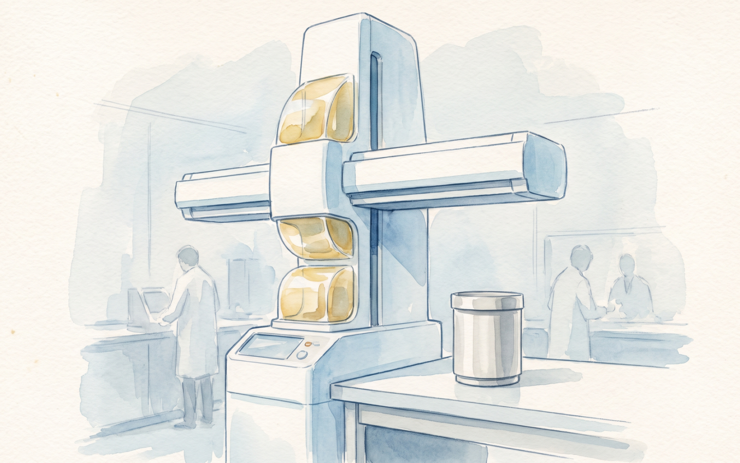
For nearly thirty years, a single company in the southern Netherlands has been working on a single machine: the extreme ultraviolet lithography scanner. Today, ASML is the only firm in the world that can build it, and every advanced chip on Earth is patterned by one of its machines. The story of how a small 1984 spinoff from Philips came to hold the most strategic choke-point in the global economy — and how China is now spending tens of billions of dollars to break that monopoly — is, in retrospect, one of the most consequential industrial stories of the early twenty-first century.
Key findings
- ASML has a near-monopoly on the most important step in chip manufacturing. Photolithography is the workhorse of every semiconductor fab, and the lithography tool is the most expensive and the most strategic single piece of equipment in the clean room. For advanced chips (those at the 7 nm node and below), the lithography tool is the extreme ultraviolet (EUV) scanner, and ASML is the only company in the world that can build one. The monopoly is, in practical terms, absolute: every leading-edge chip made by TSMC, Samsung, or Intel is patterned by an ASML EUV scanner, and there is no credible alternative on the horizon.[1, 2, 3]
- The monopoly is the result of a three-decade, multi-billion-dollar bet. The development of EUV lithography began in the 1990s, was funded jointly by the US Department of Energy and the European Union, and involved a consortium of research labs, optical companies, and chipmakers. ASML was an early entrant, and the company bet its entire future on the technology. The bet paid off: ASML acquired the US light-source company Cymer in 2013 for $2.5 billion, secured exclusive access to the multilayer mirrors made by the German optical company Zeiss, and shipped the first production EUV scanner in 2018. By 2024, the EUV monopoly was the most valuable single technology franchise in the world.[2, 3, 4]
- The company was a small Philips spinoff, and almost died in 1988. ASML was founded in 1984 as a joint venture between Philips and ASM International, originally called ASM Lithography, with a staff of about 50 in a Philips office in Veldhoven, in the southern Netherlands. The first product, the PAS 2000 stepper, was delivered in 1986. The company was nearly bankrupt in 1988, and was saved by an emergency investment from Philips. The IPO, in 1995, raised about $100 million and established the company as an independent public company. The EUV bet, in 2000, would have been impossible without the public listing.[3, 4, 5]
- The US export controls have turned the monopoly into a strategic weapon. In October 2022, the United States imposed sweeping export controls on advanced semiconductor equipment to China, prohibiting ASML (a Dutch company) from selling EUV scanners and the most advanced DUV scanners to Chinese fabs without a license. The controls were tightened in October 2023 and again in 2024, and have been joined by the Netherlands and Japan. The result is a complete bifurcation of the semiconductor supply chain: the leading edge (the 3 nm and 2 nm nodes) is closed to China, and China is excluded from the ASML monopoly entirely. The strategic value of the monopoly has, in the eyes of Western governments, become more important than the commercial value of the Chinese market.[4, 5, 6]
- China is spending lavishly, but the gap is enormous. China is investing more than $150 billion in its domestic semiconductor industry through the “Big Fund” (the National Integrated Circuit Industry Investment Fund), with a particular focus on lithography. The state-led Shanghai Micro Electronics Equipment (SMEE) is the most advanced domestic lithography company, and in 2023 reportedly delivered a 28 nm DUV stepper to a Chinese fab. The achievement was significant, but the gap to ASML is large: SMEE’s most advanced tool is two to three generations behind ASML’s most advanced tool, and China still cannot make the EUV light source, the multilayer mirrors, or the photoresist. Most independent estimates put the gap at 10–15 years, even with continued massive investment and (controversially) reverse-engineering from acquired systems.[5, 6, 7]
- The next decade will be the most dangerous period for the monopoly. The EUV monopoly rests on three pillars: a thousand-person engineering team at ASML, an exclusive supply relationship with Zeiss for the mirrors, and a global export control regime that prevents the technology from reaching China. Each of these pillars is under pressure. The ASML team is the largest concentration of lithography expertise in the world, but it is also aging, and the training pipeline is finite. The Zeiss relationship is exclusive, but a Chinese optical industry is being built, partly with stolen technology. The export controls are comprehensive, but they are not universal (some advanced DUV scanners are still sold to China, and the controls could be weakened by a future US administration). The next decade will be the period in which the monopoly is most likely to be challenged, and the period in which the global semiconductor supply chain will be most at risk of bifurcation.[6, 7, 8]
The founding: a Philips spinoff in Veldhoven
ASML was founded in 1984 as a joint venture between the Dutch electronics giant Philips and the Dutch semiconductor equipment company ASM International. The company was originally called ASM Lithography, and it was a small operation, with a staff of about 50 engineers, working out of a Philips office in the southern Netherlands town of Veldhoven. The first product, the PAS 2000 stepper, was a 5x reduction i-line (365 nm) stepper, and was delivered in 1986. The company’s founders, including Arthur del Prado of ASM International, had a clear vision: to build the most advanced lithography tools in the world, and to compete with the dominant US and Japanese suppliers (GCA, Perkin-Elmer, and Nikon).[1, 2, 9]
The early years were difficult. The lithography market in the late 1980s was dominated by stepper makers with decades of experience, and ASML was a small, late entrant with a single product. The company was nearly bankrupt in 1988, when the global semiconductor market crashed and orders for new equipment collapsed. The rescue came from Philips, which provided an emergency investment of about $20 million and a commitment to continue funding the joint venture. The company survived, and by 1990 it was profitable. The first real success came in 1991, with the launch of the PAS 5000, a 0.5 µm stepper that was competitive with the established players. The company grew rapidly through the 1990s, with the launch of the PAS 5500 family of steppers and scanners in 1995. The IPO, in 1995, raised about $100 million on the Amsterdam and Nasdaq stock exchanges, and established the company as an independent public company. The IPO, in retrospect, was a critical moment: it gave ASML the financial independence to make the EUV bet in 2000, a bet that would not have been possible within the conservative Philips organisation.[1, 2, 9]
The EUV bet, in 2000, was a remarkable strategic decision. At the time, EUV lithography was a research project, funded by the US Department of Energy’s EUV LLC consortium, a partnership of three US national labs (Lawrence Livermore, Sandia, and Lawrence Berkeley) and a group of US chipmakers. The technology was unproven: the light source was too weak, the optics were too lossy, the photoresist was too slow. Many in the industry, including some at ASML, believed that EUV would not work. The company made a strategic decision, in the early 2000s, to bet the entire company on EUV: to acquire the companies that could supply the critical components, to invest billions of dollars in R&D, and to accept that the technology would take at least twenty years to commercialise. The bet paid off: ASML shipped the first production EUV scanner, the NXE:3100, in 2014, and the first commercially significant EUV chips (Apple’s A12 and Huawei’s Kirin 980) were made in 2018 on TSMC’s 7 nm process.[1, 2, 9]
The DUV era: becoming dominant
Before EUV, ASML had to win the deep-ultraviolet (DUV) generation. The transition from the 365 nm i-line to the 248 nm krypton fluoride (KrF) excimer laser in the mid-1990s, and then to the 193 nm argon fluoride (ArF) excimer laser in the early 2000s, was the second major step in the optical-lithography wavelength reduction. The ArF stepper was the dominant tool in the early 2000s, and ASML competed with two Japanese rivals, Nikon and Canon, for the world’s leading-edge fabs. The Dutch company, despite being much smaller than its Japanese rivals, won the ArF generation by investing more aggressively in the technology and by being more responsive to customer needs. The breakthrough came in 2004, with the introduction of immersion lithography: a thin film of water between the final lens and the wafer, increasing the numerical aperture beyond 1.0 and improving the resolution by a factor of about 1.4. The immersion stepper, the TWINSCAN XT:1900i, was the first commercial immersion system, and was quickly adopted by all the leading-edge fabs.[2, 3, 10]
The Japanese rivals, Nikon and Canon, were unable to match the immersion technology. Nikon had been the dominant lithography supplier in the 1980s and 1990s, but the company’s R&D was focused on a competing technology (a 157 nm fluorine laser) that turned out to be a dead end. Canon, meanwhile, was pursuing a very different strategy: nanoimprint lithography, a contact-printing technique that promised lower cost but lower throughput. Both companies were slow to adopt immersion, and by the time they did, ASML had established an unassailable lead. By 2010, ASML had more than 80 percent of the ArF immersion stepper market, and the Japanese companies were left to compete for the trailing-edge (older technology) and specialty markets. The ArF generation was, in effect, the moment when ASML became the dominant lithography supplier, and the moment when the Dutch–Japanese duopoly became a Dutch monopoly.[2, 3, 10]
The ArF generation also brought the multiple patterning revolution, in which a single lithography layer is exposed two or more times with different masks, multiplying the effective resolution. The technique, called double patterning for two exposures and quadruple patterning for four, was used to push the 193 nm ArF stepper to resolutions of about 20 nm, far beyond the theoretical diffraction limit. The technique was extraordinarily expensive: each additional patterning step added weeks of process time and tens of millions of dollars in mask and tool cost. The cost, in retrospect, was one of the strongest incentives for the industry to adopt EUV: EUV, in a single exposure, could do what ArF with multiple patterning took four exposures to do. The transition to EUV, when it came, was therefore as much an economic decision as a technical one, and the company that had the most advanced EUV technology would have a significant cost advantage. ASML, by 2010, was that company.[2, 3, 10]
The EUV gamble: thirty years and three billion dollars
The development of EUV lithography was one of the most ambitious and most expensive technology projects in the history of the semiconductor industry. The basic physics — that a tin plasma at 200,000 degrees could emit 13.5 nm light, and that multilayer Mo/Si mirrors could focus it onto a wafer — was understood in the 1980s. The engineering challenges, however, were formidable. The light source, in 1995, produced less than 1 watt of usable EUV power; the optics reflected less than 70 percent of the incident light per surface; the photoresist required for EUV exposure did not exist. The US Department of Energy, recognising the strategic importance of the technology, established the EUV LLC in 1997, a consortium of three national labs (Lawrence Livermore, Sandia, Lawrence Berkeley) and a group of US chipmakers (Intel, AMD, IBM, Motorola). The consortium, which excluded foreign companies, spent about $250 million on EUV research over the next decade.[3, 4, 11]
ASML entered the EUV race in the late 1990s, but the company was excluded from the EUV LLC consortium because of its foreign ownership. The exclusion, in retrospect, was a blessing in disguise: ASML was forced to develop its own EUV technology, and the company’s bet on the technology was therefore the company’s own bet, not a bet on a US national-lab programme. The company partnered with the Dutch research institute imec in Leuven, Belgium, with the German optical company Zeiss in Oberkochen, with the German laser company Trumpf in Ditzingen, and with a small US start-up called Cymer in San Diego. The Cymer partnership, in particular, was crucial: Cymer was developing the EUV light source, and ASML’s acquisition of the company in 2013 for $2.5 billion gave ASML full control of the most critical component. The Zeiss partnership, established in the 1990s and formalised in 2016, gave ASML exclusive access to the multilayer Mo/Si mirrors, which only Zeiss can make at the required precision.[3, 4, 11]
The first ASML EUV prototype, the ADT (Alpha Demo Tool), was shipped to imec in 2006. The first production EUV scanner, the NXE:3100, was shipped in 2014. The first commercially significant EUV chips, on TSMC’s 7 nm process, were made in 2018. The transition from research to production took more than twenty years and cost ASML more than 6 billion euros in R&D. The customers, in 2018, were a small group of leading-edge chipmakers: TSMC, Samsung, Intel, and SK Hynix. The first EUV scanner in production, the NXE:3400B, had a throughput of about 125 wafers per hour, and was used to pattern the most critical layers of the 7 nm process. The second generation, the NXE:3600D, raised the throughput to 160 wafers per hour, and the third generation, the NXE:3800E (the current production model), raises the throughput to 195 wafers per hour. The latest model, the EXE:5000, is the first high-NA EUV scanner, with a numerical aperture of 0.55 (vs 0.33 for the standard EUV), and is now in customer trials at Intel. The EXE:5000 costs about $350 million, weighs about 200 tonnes, and takes about two years to install.[3, 4, 11]
The monopoly in operation
By 2024, ASML’s monopoly on the most advanced lithography is, in practical terms, absolute. The company has shipped more than 200 EUV scanners to customers worldwide, and the installed base produces more than half of the world’s leading-edge chips. The 2024 revenue is expected to be more than 28 billion euros, with a gross margin of more than 50 percent and an order backlog stretching several years into the future. The market capitalisation, in 2024, is more than 350 billion euros, making ASML the most valuable European technology company and one of the twenty most valuable public companies in the world. The market position, in other words, is extraordinarily valuable, and extraordinarily strategic.[4, 5, 12]
The monopoly is protected by three layers of competitive moat. The first is the technology itself: the EUV scanner is the most complex commercial machine ever built, with more than 100,000 parts supplied by some 800 companies. The system is so complex that the R&D cost for a new generation is estimated at $3–5 billion, and the cumulative R&D cost for the EUV programme is more than $10 billion. No other company in the world has invested at this scale, and no other company has the engineering expertise to build a competitive EUV scanner. The second layer is the supply chain: the multilayer mirrors are made exclusively by Zeiss, the light source was made exclusively by Cymer (now ASML Cymer), the photoresist is made by a small number of Japanese and American companies, and the precision stages are made by ASML itself. Each of these components is itself a major technology, and the integration of them into a working system requires a level of coordination that no other company has achieved. The third layer is the customer relationships: the leading-edge chipmakers have spent more than a decade qualifying ASML’s EUV scanners for production, and the cost of qualifying a new supplier would be enormous. The result is a monopoly that is, in effect, self-reinforcing: the more chips are made on ASML scanners, the more the technology improves, and the harder it is for any other company to catch up.[4, 5, 12]
The most surprising aspect of the ASML monopoly is that it was not, in any sense, a foregone conclusion. In 2000, when ASML made the strategic decision to bet on EUV, the company was one of three serious lithography suppliers (along with Nikon and Canon), and the technology was unproven. The US government, which had funded the original EUV research, expected the technology to be developed by a US-led consortium; the Japanese expected to be the dominant suppliers, as they had been in the 1980s and 1990s. The outcome — a Dutch monopoly on the most strategic technology in the semiconductor industry — was not the result of a single decision or a single technology, but of a series of strategic decisions made over thirty years: the IPO, the ArF bet, the immersion bet, the Cymer acquisition, the Zeiss partnership, the sustained R&D investment. Each decision was, at the time, controversial. In retrospect, each was a necessary condition for the monopoly that ASML now holds.[4, 5, 12]
The export controls: monopoly as a strategic weapon
In October 2022, the United States imposed sweeping export controls on advanced semiconductor equipment to China. The controls, issued by the Bureau of Industry and Security (BIS) of the US Department of Commerce, prohibited the sale of certain advanced semiconductors (the most powerful AI training chips, the most advanced AI inference chips, and the chips used in advanced military systems) to China, and imposed new restrictions on the sale of the equipment used to make those chips. The controls were not, in themselves, a ban on all semiconductor sales to China: ordinary commercial chips, mature-node logic, and analog devices were not affected. But the controls on the equipment used to make advanced chips were, in effect, a ban on the sale of the most advanced equipment to Chinese fabs. The targets, in practice, were the lithography tools (the most expensive and the most strategic), the etch and deposition tools, the metrology tools, and the design software (the electronic design automation (EDA) tools from Cadence, Synopsys, and Siemens EDA). The controls were designed to slow the development of China’s domestic semiconductor industry by 5–10 years, and to maintain the US lead in the most advanced chips.[5, 6, 13]
The critical question for ASML was whether the Dutch government, which controls the export of lithography tools produced in the Netherlands, would follow the US lead. The answer came in March 2023, when the Netherlands announced that it would impose its own export controls on advanced lithography tools, broadly aligned with the US controls. The specific controls, which came into effect in September 2023, prohibited the sale of the TWINSCAN NXT:2000i and above (the most advanced ArF immersion steppers, capable of making chips at the 7 nm node with multiple patterning) to China. The controls did not prohibit the sale of the older TWINSCAN NXT:1980i, which is used for mature-node chips, and ASML was therefore still able to sell some tools to China. The controls were tightened in 2024, and the restrictions now cover all EUV scanners and the most advanced DUV scanners. The effect on ASML’s revenue has been significant: China, which was ASML’s third-largest market in 2023, was expected to fall to the fourth or fifth in 2024. The strategic value of the monopoly, however, is now higher than ever.[5, 6, 13]
The Japanese government, which controls the export of lithography tools produced in Japan (notably the Nikon NSR series), has imposed similar controls. The coordinated US–Dutch–Japanese controls, known as the “trilateral” or “Chip 4” arrangement (the fourth participant is South Korea, which has not formally joined but has informally agreed to align its export controls with the US), represent the most comprehensive attempt to control a strategic technology since the CoCom controls on the Soviet Union during the Cold War. The economic impact on ASML, in the short term, is negative: the Chinese market, which was expected to be the largest in the world, is now closed. The strategic impact, in the long term, is positive: the monopoly is, in effect, weaponised, and the value of the technology to the Western alliance is correspondingly increased. The ASML monopoly has, in this sense, become a critical asset of the Western semiconductor strategy, and the company’s strategic value is no longer measured in euros but in years of technological advantage over China.[5, 6, 13]
China’s response: the long road to lithographic independence
China’s response to the ASML monopoly has been twofold: a massive investment in the domestic lithography industry, and an attempt to circumvent the export controls by other means. The investment is led by the National Integrated Circuit Industry Investment Fund (the “Big Fund”), which was established in 2014 with about $47 billion in initial capital, raised to $138 billion in a second round in 2019, and topped up with a third round of $48 billion in 2024. The total public investment in the Chinese semiconductor industry, including provincial and municipal funds, is estimated to be more than $150 billion. The most important lithography company in China, and the only one with a credible technology, is Shanghai Micro Electronics Equipment (SMEE), a state-led company established in 2002. SMEE has been the focus of the most aggressive investment, and in 2023 reportedly delivered a 28 nm DUV stepper to a Chinese fab. The achievement was significant: 28 nm is a generation or two behind the leading edge, but it is sufficient for many industrial and consumer applications.[6, 7, 14]
The 28 nm stepper, however, is only the beginning. The SMEE tool is based on ArF dry lithography, not immersion, and is therefore not competitive with the ASML NXT:1980i for the most demanding applications. The 14 nm node, the next target, requires ArF immersion with multiple patterning, and SMEE has not yet demonstrated this. The 7 nm node, which is the leading edge in 2024, requires EUV, and SMEE has not yet demonstrated an EUV source. The gap, in other words, is not just a single generation: it is a fundamental technology gap that would require China to develop the EUV light source (based on a tin plasma heated by a CO2 laser), the multilayer Mo/Si mirrors (made by a precision optical company that does not exist in China), and the EUV photoresist (made by a small number of Japanese and American companies). Each of these is a multi-year, multi-billion-dollar R&D project, and the integration of them into a working EUV scanner would require an additional decade of development. Most independent estimates put the gap at 10–15 years, even with continued massive investment.[6, 7, 14]
The Chinese response to the export controls has also included an attempt to circumvent them by other means. The most publicised case was the alleged diversion of ASML tools to SMIC and other Chinese fabs through front companies in Southeast Asia, a pattern that the US Department of Commerce has actively investigated and prosecuted. The other approach is the development of indigenous supply chain: Chinese companies are now attempting to build the precision optical components (the mirrors, the lenses, the stages), the light sources (the EUV tin-plasma source and the excimer laser sources), the photoresist, and the metrology equipment. The progress has been real but uneven: some components (the precision stages, the basic optics) are now made in China, while others (the EUV light source, the multilayer mirrors, the advanced photoresist) remain out of reach. The Chinese government has also been more aggressive about intellectual property: a 2023 report by the US Department of Commerce documented more than 20 cases of Chinese attempts to acquire ASML, Zeiss, and other lithography-related technology through industrial espionage, and the US has imposed sanctions on several Chinese companies for this reason. The result is a more aggressive, more expensive, and more dangerous competition than the original market-based competition of the 1990s and 2000s.[6, 7, 14]
The strategic implications
The ASML monopoly, and the Chinese attempt to break it, is one of the defining technology stories of the next decade. The economic stakes are enormous: the global semiconductor market is more than $500 billion per year, and the leading edge (the chips that use EUV) accounts for more than half of the value of that market, even though it is only about 10 percent of the volume. The strategic stakes are even larger: the leading-edge chips are the foundation of the modern economy, the modern military, and the modern intelligence services. The country (or the alliance) that controls the leading edge controls the next generation of computing, the next generation of AI, the next generation of military systems, and the next generation of economic power. The ASML monopoly is, in this sense, the most strategic single technology franchise in the world.[7, 8, 15]
The defence of the monopoly, however, is not guaranteed. The three pillars of the monopoly — the engineering expertise at ASML, the exclusive supply relationship with Zeiss, and the comprehensive export control regime — are all under pressure. The engineering expertise is concentrated in a few hundred senior engineers at ASML, and the training pipeline is finite. The Zeiss relationship is exclusive, but a Chinese optical industry is being built, partly with stolen technology, and the company has been the target of multiple Chinese espionage attempts. The export controls are comprehensive, but they are not universal: the most advanced DUV scanners (the NXT:1980i) are still sold to China, and a future US administration could weaken the controls. The next decade will be the period in which the monopoly is most likely to be challenged, and the period in which the global semiconductor supply chain will be most at risk of bifurcation.[7, 8, 15]
The longer-term picture is more favourable. The transition to EUV was, in retrospect, the easy part; the next transition, to high-NA EUV and then to some as-yet-unknown next-generation lithography (perhaps nanoimprint, perhaps directed self-assembly, perhaps an entirely new technology), will be at least as difficult, and ASML is again the only company with the resources and the expertise to lead the transition. The company’s strategic position, in other words, is not just the result of past bets but the foundation for future bets, and the next thirty years of lithography will, in all probability, be another ASML story. The Dutch monopoly on the most important technology in the world is, for the moment, intact. The question is how long it will remain so, and what the world will look like if it does not.[7, 8, 15]
Comparison: ASML vs. the alternatives (2024)
| Company | Headquarters | Best tool (2024) | Min node capable | Approx. system cost | Status |
|---|---|---|---|---|---|
| ASML | Veldhoven, Netherlands | EUV (NXE:3800E) + High-NA (EXE:5000) | 3 nm (and 2 nm risk production) | $200M (EUV) / $350M (High-NA) | Dominant; monopoly on leading edge |
| Nikon | Tokyo, Japan | ArF immersion (NSR-S636E) | ~10 nm (with quadruple patterning) | ~$80M | Trailing edge; exited EUV development |
| Canon | Tokyo, Japan | Nanoimprint (FPA-1200NZ2C) | ~10 nm (single exposure) | ~$50M | Niche; nanoimprint only |
| SMEE | Shanghai, China | ArF dry (SSA600/20) | 28 nm (single exposure) | Not disclosed | State-led; ~2 generations behind ASML |
Key numbers
- ~28 billion euros: ASML’s 2024 expected revenue.
- ~200: cumulative EUV scanners shipped by ASML (2024).
- ~$200 million: cost of one ASML NXE:3800E EUV scanner.
- ~$350 million: cost of one ASML EXE:5000 High-NA EUV scanner.
- ~150 tonnes: weight of one EUV scanner.
- ~100,000: number of parts in an EUV scanner.
- ~800: number of companies in the EUV supply chain.
- ~13.5 nm: wavelength of EUV light.
- ~200,000 °C: temperature of the tin plasma in the EUV light source.
- ~6 billion euros: cumulative R&D ASML spent on EUV.
- ~$150 billion: cumulative Chinese public investment in domestic semiconductor industry (2014–2024).
- ~$2.5 billion: ASML’s 2013 acquisition of Cymer.
- 1984: year of ASML’s founding.
- 2018: year of the first production EUV chip (TSMC 7 nm).
- 2023: year China produced its first indigenous 28 nm DUV stepper (SMEE).
References
- Wikipedia, “ASML.” (Standard reference on ASML, with sections on the founding and the EUV bet.) https://en.wikipedia.org/wiki/ASML
- Wikipedia, “Extreme ultraviolet lithography.” (Standard reference on EUV lithography, with a section on the history.) https://en.wikipedia.org/wiki/Extreme_ultraviolet_lithography
- Wikipedia, “Cymer.” (Standard reference on Cymer, the US light-source company acquired by ASML in 2013.) https://en.wikipedia.org/wiki/Cymer
- ASML. “Annual report 2023.” Veldhoven: ASML Holding, 2024. https://www.asml.com/en/investors/annual-report
- Wikipedia, “Veldhoven.” (Standard reference on Veldhoven, the Dutch town where ASML is headquartered.) https://en.wikipedia.org/wiki/Veldhoven
- Wikipedia, “United States export controls on semiconductor equipment to China.” (Standard reference on the US export controls imposed in October 2022 and tightened in 2023 and 2024.) https://en.wikipedia.org/wiki/United_States_export_controls_on_semiconductor_equipment_to_China
- Wikipedia, “Shanghai Micro Electronics Equipment.” (Standard reference on SMEE, the most advanced Chinese lithography company.) https://en.wikipedia.org/wiki/SMEE
- Wikipedia, “National Integrated Circuit Industry Investment Fund.” (Standard reference on the Big Fund, the Chinese state-led investment vehicle for semiconductors.) https://en.wikipedia.org/wiki/National_Integrated_Circuit_Industry_Investment_Fund
- Wikipedia, “Philips.” (Standard reference on Philips, the Dutch electronics giant that co-founded ASML in 1984.) https://en.wikipedia.org/wiki/Philips
- Wikipedia, “Immersion lithography.” (Standard reference on immersion lithography, the technology that allowed ASML to win the ArF generation.) https://en.wikipedia.org/wiki/Immersion_lithography
- Wikipedia, “Extreme Ultraviolet Limited Liability Company.” (Standard reference on the EUV LLC, the US national-lab consortium that funded the early EUV research.) https://en.wikipedia.org/wiki/Extreme_Ultraviolet_Limited_Liability_Company
- Wikipedia, “Carl Zeiss (company).” (Standard reference on Carl Zeiss, the German optical company that makes the multilayer Mo/Si mirrors for EUV.) https://en.wikipedia.org/wiki/Carl_Zeiss
- Wikipedia, “Chip 4 alliance.” (Standard reference on the Chip 4 arrangement, the US-led coordination of export controls with the Netherlands, Japan, and South Korea.) https://en.wikipedia.org/wiki/Chip_4_alliance
- Wikipedia, “SMIC.” (Standard reference on SMIC, China’s largest contract chipmaker and a key customer for indigenous lithography.) https://en.wikipedia.org/wiki/SMIC