The ASIC Era
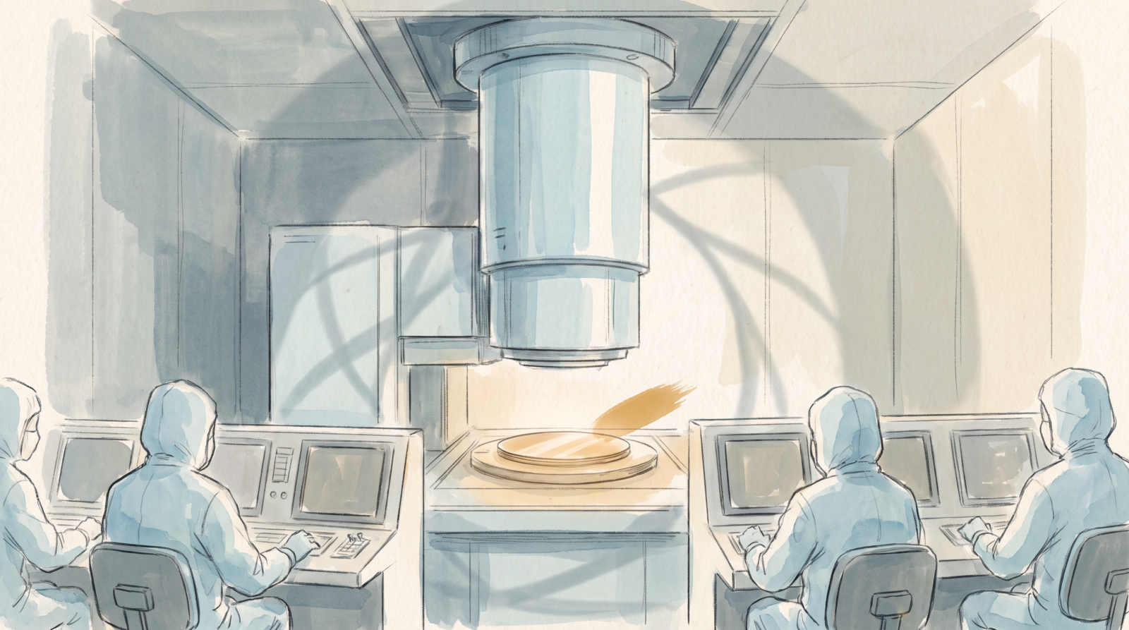
For most of the modern computing era the most interesting chips were general-purpose ones. A processor was judged by how many different kinds of work it could run, and the market for those chips rewarded flexibility. The same Intel or AMD x86 chip that ran your spreadsheet could be repurposed for a database, a web server, a video game, a compiler, a virtual machine, or a small neural network. The whole point of the design was that no one had to know in advance what the chip would be asked to do. That assumption shaped the entire industry. It shaped how chips were funded, how they were sold, how they were programmed, and how customers thought about the trade-off between performance and flexibility.
The assumption no longer holds. The center of gravity in computing has moved to one workload, matrix multiplication, and the most consequential new chips of the last five years have been designed almost entirely for that one workload. They are application-specific integrated circuits, and the period we are now in is the first one in which the most important computing systems in the world are built around them. The 2010s were the era of the GPU. The 2020s, at least so far, are the era of the ASIC.
The shift has happened in plain sight but it has not yet been named properly. The news cycle in 2024 and 2025 has mostly been about Nvidia, about OpenAI and Anthropic and Google building frontier models, and about the multi-hundred-billion-dollar commitments to compute that have followed. The new chips that have been designed for that compute have been treated as supporting characters in a story that is really about software. They are the leading characters. The decisions being made about which accelerator to use, which data format to support, which interconnect to standardise, and which memory technology to back will shape the next decade of artificial intelligence more than any single model architecture. They will also shape the industries that surround AI, because every other workload that needs serious compute is being pulled in the same direction.
The purpose of this essay is to describe the new landscape of AI-oriented application-specific silicon in enough detail to make the decisions legible. We will look at what an ASIC is and how it differs from the other kinds of chips that share its name. We will look at the history that made the current moment possible, the economics that decide who can afford to build one, the design houses that quietly design most of them, and the seven or eight specific chips and chip families that define the technological frontier. We will end with an assessment of where the architecture is going and what the next phase of the ASIC era is likely to look like.
The picture that emerges is not the picture the dominant narrative would suggest. The dominant narrative says that Nvidia has won, that the AI compute market is consolidating around a single vendor, and that the only interesting question is how big the moat gets. The technical reality is more interesting. Behind Nvidia’s commercial success is a stack of physical, economic, and software constraints that no one has resolved. The companies building ASICs for AI are not trying to beat Nvidia at its own game. They are trying to build different games.
A short note on the use of the word ASIC is in order. The term is sometimes used loosely in the trade press to mean any AI accelerator that is not a CPU. In this essay the term is used in its original sense, which is a chip designed for a specific workload, with a specific architecture, and a software stack tuned to that architecture. The GPU is, on this definition, a general-purpose accelerator rather than an ASIC, even though it is heavily optimised for AI. The TPU, Trainium, Maia, MTIA, WSE, SN40L, LPU, Blackhole, and Ascend chips are ASICs in the strict sense. The Instinct line is on the boundary. The M5, Qualcomm’s Hexagon, and Intel’s Lunar Lake client NPU are also on the boundary, but as on-device rather than data-centre parts. The distinction matters because the design, economic, and software trade-offs are different across the categories, and because the story of the ASIC era is not the same as the story of the GPU.
A second short note on the limits of what this essay can cover. The AI accelerator market is moving quickly, and several of the specific product numbers cited below, particularly for the most recently announced chips, will be revised within months of publication. The architectural story is more durable than the product numbers, and the more durable story is what this essay is trying to tell. Where specific numbers are cited from sources that are widely repeated but not independently verified, the essay tries to flag that uncertainty. Where numbers are stated as facts, they have been cross-checked against multiple sources, but the reader should still treat them as snapshots of a moving target rather than as permanent descriptions of a fixed product.
What an ASIC actually is
The acronym ASIC is older than the modern computing industry. It dates from the late 1970s and was used to describe a chip designed for a single customer, as opposed to a standard product sold to many customers. The first ASICs were gate arrays, prefabricated wafers of unconnected logic gates that a customer would specify the final interconnect pattern for. The customer paid a one-time non-recurring engineering fee, received a chip that did exactly the logic they had specified, and had no ability to change the chip after the masks were made. The economic proposition was simple. A chip that did only what you needed could be smaller, cheaper, and lower-power than a general-purpose chip that did everything for everyone.
That basic definition still holds, but the technologies that fall under it have multiplied. A modern ASIC can be a fully custom design, where every transistor is placed by hand, a standard-cell design built from a library of pre-made logic blocks, a structured ASIC that mixes hard-wired intellectual property with custom logic, a chip made from chiplets bonded together in a package, or a chip that is essentially a general-purpose processor with a specific set of accelerators bolted on. What the terms have in common is that the chip has a specific intended use, that the design effort was paid for by someone who expected to use the result, and that the chip is not sold to a broad market as a piece of generic computing equipment.
The contrast is most often drawn with three other categories. A central processing unit is a fully general-purpose sequential processor, designed to run any program that can be expressed in its instruction set. A graphics processing unit is a parallel processor designed for the kinds of matrix and vector operations that arise in computer graphics, and now widely used for AI. A field-programmable gate array is a chip whose logic can be reconfigured after manufacture, at the cost of being slower and more power-hungry than an ASIC of equivalent complexity. The relationship between these categories has shifted repeatedly. GPUs themselves started as application-specific accelerators for graphics and were only later repurposed for general parallel computing. Modern AI accelerators are ASICs by the strict definition. Modern CPUs increasingly contain specialised accelerators for AI, which makes them look a bit like ASICs nested inside a general-purpose chip. The boundary has not disappeared. It has just become a question of degree.
For the purposes of this essay, the interesting distinction is between a chip that has been designed primarily for one workload and a chip that has been designed to handle a broad class of workloads efficiently. A modern training accelerator for large language models is the first kind. A modern data-centre GPU is the second kind, even if it has been heavily tuned for AI. The distinction matters because the economic and engineering trade-offs are different. A general-purpose chip has to support a software ecosystem that cannot be changed every time the silicon is revised. An application-specific chip can be redesigned aggressively, and its software stack can be tuned to it, because the customer is locked in to a single workload anyway. The result is a wider design space, a faster iteration cycle, and a more brittle product. ASICs can be substantially better at their intended workload and substantially worse at anything else. Both halves of that statement matter.
A short history of silicon built for one job
The history of application-specific silicon is older than the AI boom. The first commercial gate arrays appeared in the late 1970s, from companies like Ferranti and LSI Logic. The early customers were mostly in telecommunications, where the volumes were high and the workloads were stable enough that custom silicon was the obvious answer. A telephone switch has to handle a known set of signalling protocols. A modem has to implement a known standard. A digital subscriber line has to encode and decode a known waveform. Building a general-purpose processor to do that work was wasteful. The first major users of ASICs were not the AI startups we associate with the term. They were the regional Bell operating companies and the equipment vendors who sold to them.
By the early 1990s, the ASIC market had matured. Cell-based design, in which a chip was assembled from a library of pre-made logic cells, had largely replaced gate arrays. Major customers included the networking equipment vendors. Cisco, Juniper, and a dozen smaller companies built almost all of their core switching and routing logic on ASICs designed in-house and manufactured by TSMC, UMC, or IBM. The first generations of high-speed Ethernet switches were ASICs. The first generation of serial ATA controllers was an ASIC. The first generation of Wi-Fi chips was, in most cases, an ASIC. The economics of building an ASIC made sense whenever a chip had to do a known job, in known volumes, at known costs. Outside those conditions, programmable processors were cheaper.
The next wave of ASICs was the one that brought the technology into ordinary consumer devices. The late 1990s and the 2000s saw a Cambrian explosion of consumer ASICs, mostly in the form of system-on-chip designs for mobile phones, set-top boxes, game consoles, and digital cameras. The original Xbox carried a custom Intel Pentium III alongside a custom Nvidia graphics chip. The iPhone, in 2007, contained an ASIC that Apple had designed at enormous expense. The first Fitbit, in 2009, contained a custom ASIC. None of these chips were called ASICs by their users, but they were ASICs by definition, and the design tools, the intellectual property libraries, and the supply chains that served them are the same ones that serve the AI market today.
The history of cryptocurrency mining is the most informative pre-AI case study. Bitcoin mining started on general-purpose CPUs, moved to GPUs for their parallel arithmetic, then to FPGAs, and finally to ASICs, between roughly 2010 and 2013. The transition was unusually fast because the workload was unusually well-defined. A Bitcoin miner had to compute a single specific hash function, the SHA-256, as fast as possible. As soon as the network difficulty rose high enough, a chip designed only for that hash function could outperform a general-purpose processor by several orders of magnitude. The first generation of Bitcoin ASICs was sold by a small number of specialised companies, of which the most famous was Butterfly Labs. The economics were familiar from earlier ASIC markets. High non-recurring engineering costs, low per-unit manufacturing costs, and a target customer base that could be identified in advance. The Bitcoin ASIC market also illustrated a problem that has returned in AI. As the network hash rate rose, the power consumption of the network rose with it, eventually reaching a point where Bitcoin mining consumed more electricity than several mid-sized European countries. The lesson, which the AI market has now had to learn for itself, is that an ASIC that makes a specific workload much cheaper to run also makes it much easier to over-provision.
The first modern AI ASIC was the Google Tensor Processing Unit, which entered production in 2016. The TPU was not the first attempt to build application-specific silicon for neural networks. The field had a long history of research chips, including the famous TrueNorth chip from IBM Research, the Neuromorphic Chip from HP Labs, and several generations of low-power inference accelerators for embedded applications. The TPU was the first commercial AI ASIC at scale. It was justified by an internal Google calculation that, given the company’s projected workload growth, a chip designed only for inference on neural networks would pay for its design costs in less than two years. The calculation was correct, and the TPU became the foundation of Google’s internal AI infrastructure for almost a decade.
The TPU was followed by a small wave of other AI ASICs. Apple’s Neural Engine, which appeared in the A11 Bionic in 2017, was the first mass-market consumer AI ASIC. Huawei’s first Ascend chip shipped in 2018. The first Habana Labs Gaudi chip appeared in 2019. Graphcore’s first Intelligence Processing Unit shipped in 2018. None of these chips displaced the GPU, but they collectively established that the AI accelerator market was a real market, that designing chips for it was commercially viable, and that a software stack, however thin, could be built around each of them. The groundwork was laid for the much larger wave that began in 2022.
The economics of being specific
The decision to design an ASIC is fundamentally an economic decision. The design effort, the mask cost, the qualification, the software stack, and the verification all have to be paid for up front, in advance of any revenue. The total cost of a modern AI ASIC is hard to estimate from public disclosures, but the order of magnitude is clear. A leading-edge logic design at the 3-nanometre node costs several hundred million dollars in engineering effort over a two-to-three-year development cycle. The mask set alone, the photomasks used to print each layer of the chip, costs between thirty and one hundred million dollars at the most advanced process nodes. The software stack, which is the largest single component of the total cost, easily runs to several hundred million dollars more. The result is that an AI ASIC at the leading edge is a billion-dollar bet before the first chip is sold.
This is the single most important fact about the industry. It explains who can afford to design AI ASICs and who cannot. The companies that have shipped leading-edge AI ASICs in 2024 and 2025 are, with very few exceptions, companies that already had a customer for the chip before the design started, and a workload that could justify the cost. Google, Amazon, Apple, Huawei, Meta, Microsoft, and Tesla are all in this category. The independent AI ASIC companies that have reached production, including Cerebras, SambaNova, Groq, and Tenstorrent, are exceptions that mostly confirm the rule. Each of them has a smaller, more specialised target workload than the hyperscalers, which lets them design a smaller, cheaper chip and amortise the cost over a smaller customer base. Even so, the cost of staying at the leading edge is a constant constraint on their growth.
The economics of being specific are not entirely prohibitive. Several trends have lowered the cost of entry. The first is chiplet-based design. Modern advanced packages can hold multiple smaller chiplets bonded together, each of which can be manufactured on a process node appropriate to its function. The most aggressive early users of this approach, including AMD in its Epyc and Instinct lines and Apple in its M-series chips, have shown that a chiplet design can match or exceed the performance of a monolithic design at substantially lower cost. The second trend is the maturation of the open instruction set RISC-V, which lets a new entrant use a free, well-maintained processor core instead of paying the licensing fees for an Arm or x86 core. The third trend is the rise of the third-party design house. Companies like Broadcom, Marvell, Alchip, Global Unichip, Synopsys, and Cadence now offer turnkey ASIC design services that can take a customer’s algorithm and produce a working chip, including the software stack, for a fraction of the cost of an in-house design.
The third-party design services are probably the most important of these trends. A company that wants a custom AI chip today can in principle walk into Marvell or Broadcom with a model specification and walk out with a packaged, tested silicon two years later, for a price somewhere between fifty and several hundred million dollars. The economics are still demanding but they are no longer exclusive to the hyperscalers. The trend is one of the reasons that the current ASIC boom is so much larger than the early 2000s ASIC boom. In 2003, only the biggest equipment vendors could afford a custom chip. In 2026, mid-sized companies with a few hundred million dollars of capital can afford one too.
The hidden cost is software. A modern AI accelerator is not just silicon. It is also a compiler, a kernel library, a runtime, a debugger, a profiler, an integration with PyTorch and TensorFlow, an integration with Hugging Face, and increasingly an integration with a model-serving framework like vLLM or TensorRT-LLM. Building this software stack from scratch is what kills most AI ASIC companies. It is the part of the work that the AI research community has done for free, and the part that every new entrant has to replicate. Cerebras, SambaNova, Groq, and Tenstorrent have all spent more on software than on silicon. The companies that have succeeded are the ones that built a software stack comparable in scope to what Nvidia built around CUDA over fifteen years, in a fraction of the time, with a fraction of the headcount. The cost of that software is the single most underappreciated reason that the AI ASIC market is not larger than it is.
FPGAs, ASICs, and the middle ground
The field-programmable gate array, or FPGA, sits between the general-purpose processor and the ASIC. An FPGA is a chip whose logic and interconnect can be reconfigured by loading a new pattern of bits into the chip’s configuration memory. The configuration takes a few milliseconds. Once configured, the chip behaves like an ASIC built out of the resources the FPGA provides. A typical modern FPGA contains hundreds of thousands of lookup tables, hundreds of digital signal processing blocks, blocks of static random access memory, high-speed transceivers, and one or more hard processor cores. The largest FPGAs from AMD’s Xilinx line and from Altera, now part of Intel, contain several million logic elements and several tens of megabytes of on-chip memory.
FPGAs have been used for AI workloads since the early 2010s. Microsoft was an early and large customer, using Altera and Xilinx FPGAs in its Bing ranking infrastructure and in its data-centre network. The economics were familiar from the ASIC story. An FPGA is slower and more power-hungry than an ASIC of equivalent logic capacity, by roughly a factor of three to five on a per-operation basis, but it can be reconfigured for new workloads and reused across many deployments. For low-volume or rapidly evolving workloads, the flexibility is worth the efficiency penalty. For high-volume stable workloads, it is not.
The current generation of AI ASICs has, to a large extent, displaced the FPGA for production AI workloads. The reasons are partly performance, partly unit cost, and partly the rise of chiplet-based design, which has narrowed the flexibility advantage of the FPGA. There are still niches in which FPGAs make sense, particularly at the network edge, where the workload changes often and the volume is too low to justify an ASIC, and in the academic and research community, where FPGAs are still used for novel AI architectures. For most production AI workloads, however, the FPGA has been supplanted by chips that are either application-specific or that lie at the very edge of the general-purpose category, like the AMD Instinct accelerators, that are themselves a kind of structured ASIC for AI.
The memory wall and the physical limits
Every AI accelerator, whether it is a GPU, an ASIC, or an FPGA, is constrained by the same physical limit. The amount of data that can be moved between the memory and the compute units, per second, is bounded by the bandwidth of the memory system and the interconnect. A modern AI training run involves roughly ten to twenty floating-point operations for every byte of data that has to be moved, and the ratio has been declining for years. The classical formulation of the problem, the memory wall, has been known since the 1990s, and the AI boom has turned it from an academic concern into a binding constraint on the entire industry.
The dominant solution to the memory wall is high-bandwidth memory, or HBM. HBM stacks multiple DRAM dies vertically and connects them to a logic die through a silicon interposer using through-silicon vias. The current generation, HBM3e, delivers roughly one terabyte per second of bandwidth per stack, and a single accelerator can hold several stacks. HBM4, which began shipping in 2026, roughly doubles the per-stack bandwidth again. The cost is correspondingly high. HBM is one of the most expensive components in any modern AI system, and the supply is tightly constrained. All three major suppliers, Samsung, Micron, and SK Hynix, are sold out through 2027.
The packaging that holds the logic die, the HBM stacks, and any other chiplets together is a second constraint. The dominant technology is TSMC’s Chip-on-Wafer-on-Substrate, or CoWoS, which uses a silicon interposer to bond the components into a single package. The demand for CoWoS capacity has tripled in the last two years and is still growing. Nvidia holds an estimated sixty per cent of the 2026 CoWoS supply, and the top three customers, Nvidia, Broadcom, and AMD, together hold more than eighty-five per cent. The capacity is being expanded, but the lead time for the most advanced CoWoS variants is reported at between fifty-two and seventy-eight weeks, which is longer than the design cycle of a typical AI ASIC.
A third, less appreciated constraint is the substrate material used in the CoWoS package. The so-called ABF substrate, an organic interposer made of a glass-fibre-reinforced epoxy, is dominated by a single Japanese supplier. The substrate is the second most capacity-constrained input in the AI supply chain after HBM, and analysts expect the supply gap to widen from roughly ten per cent in the second half of 2026 to forty-two per cent by 2028.
The implication for ASIC design is direct. A chip can be designed in software and laid out in a few months. The physical instantiation of that design, in the form of a packaged, tested, working chip, is a multi-quarter, multi-vendor operation that depends on the availability of advanced packaging and HBM. The companies that have secured long-term allocations of CoWoS and HBM capacity, including Nvidia, Broadcom, AMD, Google, and Amazon, have a structural advantage over those that have not. The independent ASIC companies have to compete for whatever capacity is left.
The design houses behind the chips
Most of the AI ASICs described in this essay are not designed by the company whose name is on them. They are co-designed with one of a small number of contract design houses that have accumulated the expertise, the tools, and the relationships with TSMC that are required to bring a leading-edge chip to market. Broadcom is the most visible of these houses. It has co-designed every recent generation of Google’s Tensor Processing Unit. It co-designs Meta’s MTIA. It does custom ASIC work for several of the major Chinese hyperscalers. Its annual AI-related revenue runs into the tens of billions of dollars, much of it from chips that ship under other people’s brand names.
Marvell is the second major design house. Marvell’s custom-silicon business is built around an intellectual property portfolio that includes high-speed SerDes interfaces, die-to-die interconnects, silicon photonics, advanced packaging expertise, and a growing collection of application-specific compute fabrics. Marvell designs custom XPUs for several large customers and is the partner of choice for hyperscalers that want a high-performance accelerator without building the design team in-house. In 2025, Nvidia invested two billion dollars in Marvell as part of a strategic partnership under which Marvell-designed accelerators can be integrated with Nvidia’s NVLink rack-scale systems. The investment is one of the most strategically interesting moves in the entire ASIC era, because it pulls one of the most important third-party design houses into Nvidia’s proprietary interconnect ecosystem.
Other significant design houses include Alchip Technologies, which has been particularly active in the Japanese and Taiwanese markets, Global Unichip, which is the largest pure-play ASIC design house in Asia, and the electronic design automation vendors Synopsys and Cadence, which provide the synthesis and verification tools on which every modern chip depends. The rise of these design houses has been one of the most important developments in the semiconductor industry over the last decade. They have lowered the barrier to ASIC design, allowed a much larger set of customers to build custom silicon, and shifted the centre of gravity in the industry from a few large vertically integrated companies to a more distributed ecosystem in which design expertise is available on a contract basis.
The most important consequence is that the boundary between an AI ASIC and a custom XPU is now almost meaningless. Every AI ASIC is, at some level, a custom XPU, and every custom XPU is, at some level, an AI ASIC. The naming is a marketing convention, not a technical one. What matters is the specific architectural choices a given chip has made, and the workload it has been designed for.
Cerebras and the wafer-scale bet
Cerebras Systems has pursued the most aggressive of the architectural bets in the current ASIC era. Where every other AI accelerator is a chip, Cerebras has built what is, in effect, a wafer. The Wafer Scale Engine 3, announced in March 2024, occupies roughly 46,225 square millimetres of silicon, the size of a dinner plate and more than fifty times the area of a leading-edge GPU. The chip integrates four trillion transistors, nine hundred thousand AI cores, forty-four gigabytes of on-chip static random access memory, and a fabric bandwidth of 214 petabits per second. The memory bandwidth is roughly seven thousand times that of an Nvidia H100. The peak AI compute is 125 petaflops in highly sparse FP16.
The engineering bet is that the memory bandwidth problem, which is the binding constraint on every other AI accelerator, can be solved by putting all of the memory on the same piece of silicon as the compute. By eliminating the off-chip interconnect, Cerebras avoids the bandwidth bottleneck that defines the GPU. The 21 petabytes per second of memory bandwidth that the WSE-3 provides is enough that any modern AI model can be stored entirely in the on-chip SRAM and accessed at full speed. The CS-3, the system built around the WSE-3, can train a one-trillion-parameter model as easily as it trains a one-billion-parameter model, because the entire model fits in memory.
The wafer-scale approach is not without cost. A single WSE-3 die is too large to be manufactured with any reasonable yield. Cerebras compensates by accepting that many of the cores on the wafer will be defective at manufacture and by mapping workloads around the defects. The company has also invested in a custom packaging and cooling system that allows the wafer to be operated at full power. The CS-3 system draws roughly 23 kilowatts, comparable to a high-end GPU server but with substantially more compute per watt. The largest Cerebras deployment is the Condor Galaxy 3 in Dallas, which combines 64 CS-3 systems into a single 8-exaflop supercomputer, and which is used primarily for training the largest available open-source models.
Cerebras’s most visible commercial move in 2025 was a partnership with Qualcomm to combine Cerebras-trained models with Qualcomm’s datacenter inference chips. The partnership is a tacit acknowledgement that Cerebras’s wafer-scale approach is unlikely to displace the GPU in the general-purpose training market, and that the company’s commercial future is more likely to be in high-speed inference and in the long tail of large model training jobs that do not fit cleanly into the GPU’s batch-parallel model. The company has also moved aggressively into the inference market, claiming speeds of 1,800 tokens per second on Llama 3.1 8B and 450 tokens per second on Llama 3.1 70B, roughly twenty times faster than GPU-based alternatives at one-third the power.
SambaNova and the dataflow alternative
SambaNova Systems has taken a different bet, which is that the GPU is the wrong abstraction entirely. The fourth-generation SambaNova chip, the SN40L, is built around a Reconfigurable Dataflow Unit, or RDU, that does not look like a GPU at all. The chip has 1,040 cores, each containing a small programmable compute unit and a memory management unit, connected by a mesh network with three separate physical planes for data, addresses, and control. The chip carries 520 megabytes of on-chip SRAM, 64 gigabytes of high-bandwidth memory, and up to 1.5 terabytes of additional DDR memory. The total compute is 638 teraflops in BF16 precision, which is roughly an order of magnitude less than a leading-edge GPU at the same precision.
The dataflow architecture is designed to avoid the inefficiency of GPU kernel launches. On a GPU, every operation, including the matrix multiplications, the normalisations, the activations, and the memory copies, has to be launched as a separate kernel. The launch overhead is small for any one kernel but adds up to a substantial fraction of the runtime for inference. The dataflow architecture fuses all of the operations in a model layer into a single graph that runs without kernel launches. The result is that the same model runs several times faster on a SambaNova system than on a GPU, and that the same rack can run several models simultaneously, switching between them in tens of milliseconds.
The most distinctive claim from SambaNova is its hot-swapping capability. The three-tier memory architecture, with 520 megabytes of SRAM, 64 gigabytes of HBM, and up to 1.5 terabytes of DDR per chip, means that a single rack can hold dozens of models resident in memory at once. The system can switch between them in sixty to ninety milliseconds, which is roughly an order of magnitude faster than the equivalent operation on a GPU. The capability is particularly useful for agentic AI, where a single application may need to use several different models, including a small one for routing, a medium one for tool use, and a large one for the heavy thinking steps. On a GPU, switching between models takes hundreds of milliseconds to seconds. On a SambaNova system, it is essentially free.
The system is sold as the SambaRack, which contains 16 RDUs, draws between 7 and 14 kilowatts at typical load, and supports up to 5 trillion parameters of resident models. The energy efficiency is also distinctive. SambaNova claims between four and nine times better performance per watt than the Nvidia H200 in common inference workloads, and the company is one of the few AI ASIC vendors that has aggressively marketed its products on energy efficiency rather than peak performance. The combination of fast switching, low power, and high energy efficiency is a more compelling story for enterprise deployment than for hyperscale training, and SambaNova has accordingly concentrated on the enterprise market.
Groq and the deterministic bet
Groq has made the most unusual architectural choice in the current ASIC era, which is to abandon the conventional processor memory hierarchy entirely. The Language Processing Unit, or LPU, that Groq sells, has no high-bandwidth memory, no large on-chip SRAM, and no cache. Instead, it integrates 230 megabytes of on-chip static memory that holds the entire model and from which weights are fed to the compute units at a rate of 80 terabytes per second, roughly twenty times faster than the bandwidth of an HBM stack.
The architectural bet is that, for inference, determinism matters more than flexibility. The LPU uses a programmable assembly-line architecture in which the compiler knows exactly when every weight and every activation will arrive at every compute unit. There is no scheduling, no caching, no branch prediction, and no memory hierarchy to manage. The execution time of a model is fully predictable to the clock cycle, and the latency for a single token is roughly an order of magnitude lower than the equivalent operation on a GPU. Groq’s published benchmarks include Llama 2 70B at 300 tokens per second per user, which is roughly ten times faster than a comparable H100 deployment.
The LPU is not without cost. A single LPU has roughly 188 teraflops of FP16 compute, which is comparable to a single GPU from several years ago, and is much less than a current top-end GPU. Running a model larger than what fits in 230 megabytes of SRAM requires many LPUs working together, and the inter-chip communication protocol that Groq has developed to coordinate them, called plesiosynchronous, is unusual enough to require special hardware. Running a 70-billion-parameter model requires roughly 576 LPUs working as a single logical core. The system is more expensive per unit of throughput than an H100 cluster, by a factor of roughly two to four, depending on the model and the workload.
The commercial positioning of Groq has accordingly focused on low-latency inference, where the unit economics of a fast LPU are more favourable than they would be in a throughput-sensitive training workload. GroqCloud, the company’s hosted inference service, has more than 1.9 million developers and enterprise customers including Dropbox, Volkswagen, and Riot Games. In April 2025 Groq signed a partnership with Meta to provide inference for the official Llama API, and in October 2025 Groq signed a strategic partnership with IBM to integrate GroqCloud with IBM’s watsonx Orchestrate platform. Both partnerships are aimed at the inference market rather than training. Groq does not support training, and is unlikely to.
A separate strand of the Groq story is the recent partnership with Nvidia, under which a future generation of Groq LPU is to be integrated with Nvidia’s Vera Rubin systems as a low-latency inference coprocessor. The partnership is the most concrete evidence that Nvidia sees the LPU class of accelerator as a complement to its own GPUs rather than a competitor, and that the future of AI compute will be a heterogeneous mix of accelerator types working together.
Tenstorrent and the open bet
Tenstorrent, a Toronto and Santa Clara company led by the chip architect Jim Keller, has bet on an entirely different foundation. Where every other AI accelerator in the current generation is a proprietary architecture, Tenstorrent’s chips are built on the open RISC-V instruction set, with a fully open-source software stack, and are sold both as physical hardware and as licensable design intellectual property. The bet is that the AI hardware market will eventually resemble the broader CPU market, in which a free, well-maintained instruction set, supported by a wide ecosystem of independent vendors, eventually displaces any single proprietary architecture.
The current Tenstorrent silicon is the Blackhole generation, launched in April 2025. Each Blackhole chip contains 140 Tensix cores, each of which integrates five small in-house RISC-V control cores, a vector unit, a matrix unit, and roughly 1.5 megabytes of local SRAM. The chip also integrates 16 SiFive X280 RISC-V cores that can run Linux directly, which means that a single Blackhole chip can function as a standalone AI computer without a separate host processor. The peak compute is 745 teraflops in FP8, the memory is 32 gigabytes of GDDR6 at 512 gigabytes per second, and the board power is roughly 300 watts. The list price for a single-card Blackhole is 1,399 dollars, and a fully configured 32-chip Galaxy server is 110,000 dollars.
The architectural bet is that programmability matters. A Tensix core is, in effect, a small computer in its own right, with its own instruction streams and its own local memory. The five RISC-V cores per Tensix tile handle the data movement, the unpacking and packing of data, and the issuance of compute operations, while the matrix and vector units do the actual arithmetic. The result is a chip that is more programmable than a GPU but more efficient than a CPU. The trade-off is that peak performance per chip is lower than a leading-edge GPU, and that the software stack, while open, is less mature than CUDA.
The open-source angle is also a bet. Tenstorrent’s entire software stack, including the low-level TT-Metalium environment, the TT-Forge compiler, and the TT-Buda model deployment tool, is published under permissive open-source licenses. Customers can read the code, modify it, and contribute back. The argument is that an open ecosystem will, over time, develop a larger community of contributors than any single vendor can afford to hire, and that the resulting software stack will eventually be more capable than the closed stacks that Nvidia, AMD, and the hyperscalers maintain internally. The argument is plausible. It is also a long-term bet, and the AI hardware market has not historically rewarded long-term bets.
Lightmatter and the photonic bet
Lightmatter has made the most radical architectural bet in the current ASIC era, which is to replace the electrical interconnect between compute units with optical interconnect, and eventually to replace the compute units themselves with optical analogues. The company was founded in 2017 with the thesis that the bandwidth, latency, and energy problems of conventional AI accelerators are not solvable by better electrical design alone, and that the only way to continue scaling performance is to move to photons.
The first commercial Lightmatter product was the Passage interconnect, a chip that integrates optical transceivers and a programmable waveguide network on the same die. The most recent version, the Passage M1000, delivers 114 terabits per second of total optical bandwidth, occupies roughly 4,000 square millimetres in a 3D-stacked package, and supports 256 optical fibres at the package edge. The product is not a compute accelerator. It is a chip-to-chip interconnect that lets several conventional accelerators share memory and data at much higher bandwidth than electrical links can provide. The M1000 began sampling in 2025 and is targeted at hyperscale AI deployments that have hit the limits of conventional NVLink and Infinity Fabric.
The second Lightmatter product was the Envise photonic AI accelerator, which performed matrix multiplications by manipulating light through a mesh of Mach-Zehnder interferometers. The chip was the subject of a peer-reviewed paper in Nature in April 2025, which demonstrated that photonic matrix multiplication can run state-of-the-art neural networks to near-electronic precision. The chip integrated four photonic tensor cores, each performing 128-by-128 matrix-vector products in a single optical pass, and ran at roughly 65.5 tera operations per second per package, which is a respectable number for a first-generation product but well below a leading-edge GPU. The Envise chip is, however, no longer commercially marketed. The company has pivoted to the Passage interconnect, on the pragmatic grounds that the bottleneck in the current generation of AI systems is not matrix multiplication but rather communication between chips, and that a photonic interconnect is a more immediate commercial opportunity than a photonic compute unit.
The pivot is a useful illustration of the discipline required to survive in the ASIC market. Lightmatter had a working photonic compute chip. It also had a working photonic interconnect. The interconnect was the easier sell, because it could drop into existing systems without requiring a new software stack, a new memory hierarchy, or a new model-serving framework. The compute chip, however elegant, would have required all of those. The company’s bet that the future of AI hardware will include photonic components remains intact, and the Passage L20, a near-package optics interconnect announced in March 2026, is the most recent evidence of that bet. But the bet is being made in interconnect first, and in compute second, which is the opposite of the order in which most AI accelerator companies have made their bets.
AMD and the second-tier general-purpose
The AMD Instinct line is the most commercially successful of the AI accelerators that is not made by Nvidia, and the one that most clearly does not fit the strict definition of an ASIC. The Instinct MI300X, launched in December 2023, integrates 304 compute units, 192 gigabytes of HBM3 memory at 5.3 terabytes per second, and 153 billion transistors on a TSMC 5-nanometre process. The successor, the MI325X, increases the memory to 256 gigabytes of HBM3e at 6 terabytes per second. The MI350X and MI355X, which began shipping in mid-2025, are built on a 3-nanometre process, support the FP4 and FP6 data types that Nvidia’s Blackwell generation introduced, and carry 288 gigabytes of HBM3e at 8 terabytes per second. The MI400 series, expected in 2026, is built on the next CDNA architecture and is intended to compete with Nvidia’s Vera Rubin generation.
The Instinct accelerators are not ASICs in the strict sense. They are general-purpose GPUs with the graphics hardware removed and the AI hardware path optimised. They use the ROCm software stack, which is AMD’s open-source competitor to CUDA, and they support the same broad set of AI workloads as Nvidia’s hardware, including training, inference, recommendation systems, and scientific computing. The architectural approach is therefore different from that of Cerebras, SambaNova, Groq, Tenstorrent, Lightmatter, or the hyperscaler in-house designs. AMD is competing in the general-purpose category, where the customer expects to be able to run any model on the hardware without a custom porting effort.
The commercial success of the Instinct line has been substantial. AMD’s data-centre revenue grew from roughly six billion dollars in 2023 to more than twelve billion in 2024 and is on track to exceed twenty billion in 2025. The MI300X in particular has been adopted by Microsoft for some of its OpenAI workloads, by Meta for parts of its recommendation infrastructure, and by a long tail of enterprises that wanted a second source for AI compute. The MI325X and MI350X are likely to capture further market share as enterprises and hyperscalers seek to reduce their dependence on a single supplier.
The interesting question for the ASIC era is whether AMD’s general-purpose approach will continue to scale. The history of the GPU market suggests that the answer is yes. General-purpose accelerators have a long-term advantage in software ecosystem that is hard for narrower products to overcome. But the history of the ASIC market also suggests that there is a class of workloads, particularly large-scale inference, where the narrower product wins. AMD’s challenge in 2026 and beyond is to hold the general-purpose middle of the market while the hyperscalers and the independent ASIC companies take the extreme ends.
Huawei Ascend and the constrained-design path
Huawei’s Ascend line is the most important AI ASIC that is not designed in the United States or Europe. The chip family has been under continuous US export controls since 2019, which has forced Huawei to design for foundries that are not subject to the controls, namely SMIC, the largest Chinese foundry, and to do without the most advanced photolithography equipment. The first Ascend chip, the Ascend 910, was manufactured by TSMC on the N7+ process in 2019. The current generation, the Ascend 910B, is manufactured by SMIC on a 7-nanometre-class process that uses deep ultraviolet lithography rather than the more advanced extreme ultraviolet lithography. The next generation, the Ascend 910C, packages two 910B dies into a single component. The 910C delivers roughly 800 teraflops of FP16 performance, 128 gigabytes of HBM, and 3.2 terabytes per second of memory bandwidth, all on a process node that is roughly two generations behind the leading edge.
The numbers are not competitive with Nvidia’s leading-edge parts on a per-chip basis. The 910C is roughly comparable to a two-generation-old Nvidia GPU. What the Ascend line has done is to compensate for the per-chip deficit by building very large systems. The CloudMatrix 384, announced in 2025, combines 384 Ascend 910C chips into a single rack-scale system, with 6,912 400-gigabit silicon photonic optical links providing 2.8 terabits per second of bandwidth per chip. The system delivers roughly 300 petaflops of FP16 performance, which is competitive with a large Nvidia GB200 cluster. The Atlas 900 A3 SuperPoD, which builds on the CloudMatrix 384, has been deployed at more than 1,000 sites in China as of September 2026, serving more than 20 customers.
The Ascend line illustrates what constrained design can do. Without access to the most advanced foundries, the most advanced packaging, or the most advanced high-bandwidth memory, Huawei has built a competitive AI accelerator family by accepting lower per-chip performance and using systems engineering, optical interconnect, and very large chip counts to reach competitive system-level performance. The approach is not a substitute for the leading edge. It is a different way of reaching the same destination, and it is the model that other constrained buyers, including the Chinese hyperscalers, the Russian sovereign cloud, and parts of the European public sector, are likely to copy.
The other interesting feature of the Ascend line is the software. The CANN compute architecture and the MindSpore framework are Huawei’s answer to CUDA and PyTorch, and they are the part of the programme on which the most investment has been made. The software is good enough to support large-scale training, but it is not good enough to make Ascend competitive outside the Chinese market, where the alternatives are unavailable. The lesson, which has been repeated by every other AI ASIC company, is that the software is the hardest part.
Apple silicon and the on-device angle
Apple’s M-series chips are the largest-volume AI ASICs in the world by units shipped, and the only ones that most consumers will ever interact with directly. The M5, released in October 2025, is built on TSMC’s third-generation 3-nanometre process and integrates a 10-core CPU, a 10-core GPU with a dedicated Neural Accelerator in every GPU core, a 16-core Neural Engine, and 153 gigabytes per second of unified memory bandwidth. Apple claims more than four times the peak GPU compute for AI compared to the M4, and roughly 3.5 times the AI performance in real-world workloads.
The M5 is not designed for hyperscale training. It is designed to run AI models on a laptop. The on-device AI use case is fundamentally different from the hyperscale training use case. The model has to fit in tens of gigabytes of memory rather than hundreds of gigabytes. The user is a single person rather than a fleet of customers. The latency has to be low enough to feel instantaneous, and the battery has to last a working day. None of these constraints matter for the hyperscale training market. All of them matter for the on-device market.
The on-device angle is, in some ways, the most interesting part of the ASIC era. The vast majority of the public conversation about AI compute is about the hyperscale training market, where the chips cost tens of thousands of dollars each and the systems cost hundreds of millions. The on-device market is the larger market by units, and it is the one that most directly affects the user experience of AI. Apple’s bet, like Qualcomm’s, is that a substantial fraction of AI inference will eventually move from the cloud to the device, and that the device will need a chip designed for that specific workload.
The bet has not yet paid off in any obvious way. The current generation of on-device AI features, including Apple Intelligence and the equivalent features on Windows and Android, still rely heavily on cloud inference. But the on-device inference market is growing, and the chips that will run it are being designed now. The M5 is one of them. Qualcomm’s AI 100 Ultra is another. Intel’s Lunar Lake and Arrow Lake client platforms, with their integrated neural processing units, are a third. The on-device ASIC market is, in its own way, as significant as the hyperscale ASIC market, and it is much less well covered in the trade press.
The bets that did not pay off
The visible companies in the ASIC era tend to be the ones that have survived. The companies that did not are less visible, and their stories are more instructive than the success stories, because the failures show what does not work in the AI ASIC market. The most important common feature of the failures is software. The second most important is the size of the addressable market relative to the size of the engineering investment. The third is the difficulty of competing with a general-purpose alternative that is good enough for almost everyone.
Graphcore is the highest-profile failure of the first AI ASIC wave. The Bristol-based company raised more than 700 million dollars between 2016 and 2020, and produced three generations of the Intelligence Processing Unit, a chip that used a bulk synchronous parallel programming model to coordinate thousands of small cores. The architecture was unusual, the company published impressive benchmark numbers, and the management was widely respected. By 2022, however, the company was struggling to find customers at scale. The software stack, called Poplar, never reached the maturity of CUDA, and the workloads that the IPU was best at turned out to be narrower than the company had projected. In July 2024 Graphcore was sold to SoftBank, reportedly for less than 600 million dollars, a substantial markdown on the most recent private valuation. The intellectual property is now part of SoftBank’s portfolio and may yet re-emerge in a different product, but as a standalone AI ASIC company Graphcore is finished.
Wave Computing was an earlier failure, and a more complete one. The company, founded in 2010, was one of the first to use a dataflow architecture for deep learning inference, and was awarded a DARPA contract in 2017 to build a dataflow-based AI supercomputer. The contract was cancelled in 2019, the company filed for bankruptcy later the same year, and the assets were acquired by a Chinese cryptocurrency mining company called Tallwood. The story illustrates how a technology can be technically impressive, even genuinely useful, and still fail commercially. The market for a dataflow inference accelerator in 2018 was just too small to support a billion-dollar company, and the dataflow approach did not yet have a clear customer.
Mythic AI is a more recent and less final failure. The company, founded in 2012, raised more than 165 million dollars to build an analog in-memory compute engine that stored neural network weights in the gate capacitance of flash memory cells. The architecture was genuinely novel, the engineering was impressive, and the company published benchmark numbers that looked competitive with low-power inference GPUs. The challenge was that the analog computation was hard to scale to the precision required for modern transformer models, and that the customers the company targeted, including the major consumer electronics brands, were unwilling to commit to a single-vendor analog accelerator when software-programmable alternatives were available at similar cost. Mythic has had several rounds of layoffs and pivots, and the company is now a much smaller business than its venture capital investors once hoped.
The Intel Habana story is the most instructive of the failures, because the engineering and the customer relationships were both there. Intel acquired the Israeli AI accelerator company in 2019 for roughly 2 billion dollars, and the Habana team shipped three generations of the Gaudi accelerator between 2020 and 2024. The architecture was competitive, the integration with Intel’s foundry and packaging capabilities was excellent, and the company had access to a deep customer base through Intel’s traditional sales channels. None of it mattered. CUDA compatibility, real or perceived, was the binding constraint on enterprise adoption, and the Gaudi software stack never reached the maturity required to displace Nvidia in the most lucrative workloads. In 2025 Intel effectively ended the standalone Gaudi programme and folded the engineering work into a broader effort to build custom AI chips for specific internal and external customers. The hardware is still being designed. The product line as it was originally conceived is gone.
Qualcomm’s AI 100 accelerator is a more ambiguous case. The company has shipped several generations of the chip, has a deep customer base in the mobile market, and has the resources to keep investing. But the AI 100 has not been a commercial success at anything close to the scale of the Cloud AI 100 effort, and the company’s strategic focus has shifted to the Hexagon neural processing unit integrated into the Snapdragon client platforms. The lesson is that an AI ASIC can succeed as a component of a broader system-on-chip even when it fails as a standalone accelerator.
The pattern across these failures is consistent. The most important predictor of failure is not the quality of the silicon, the novelty of the architecture, or even the size of the engineering team. The most important predictor is whether the company can build a software stack that is good enough to make the chip usable for the workloads the customer actually has, and whether the workload is large enough to justify the cost of the chip. The first failure mode is technical, the second is economic, and both have to be avoided for an AI ASIC company to survive.
When the model and the silicon co-evolve
A subtler and more recent change in the ASIC era is that the design of the silicon and the design of the AI models are no longer independent. The earliest AI ASICs were designed to run models that already existed, including convolutional networks for image classification and recurrent networks for speech recognition. The chips had to be general enough to handle a wide range of architectures, and the software stack had to support the existing model frameworks. The chips that won, including the TPU and the early Gaudi parts, were the ones that handled the broadest range of existing models the fastest.
The current generation of AI ASICs is being designed for a different world. The most important models of 2025 and 2026 are large language models, and the most important new architectural features inside those models, including mixture-of-experts, sparse attention, and state-space models, are being designed with specific hardware features in mind. The MoE architecture, in which only a small fraction of the model’s parameters are active for any one input, is naturally suited to a chip that can allocate compute to the active experts without paying the cost of computing on the inactive ones. The sparse attention pattern, in which each token in a sequence attends to only a fraction of the other tokens, is naturally suited to a chip that can support fine-grained data-dependent sparsity in the matrix multiplication unit. State-space models, which have a fundamentally different pattern of memory access than transformers, are naturally suited to a chip that has a different balance of compute and memory bandwidth.
The co-evolution has gone both ways. The Google research team behind Gemini has published several papers on model architectures that are explicitly designed to take advantage of TPU features. The SambaNova team has published a paper arguing that the dataflow architecture is uniquely well-suited to MoE models, and has built a version of the company’s software stack around that claim. The Groq team has argued that the deterministic LPU architecture is well-suited to agentic systems, in which the latency of an individual model call is more important than the throughput of the system. None of these claims is fully proven, but all of them are being tested in production.
The long-term implication is that the boundary between the silicon and the model is becoming more porous. The next generation of frontier models will, in many cases, be designed to take advantage of specific features of specific chips. The most important AI labs are now maintaining teams that work on both sides of the boundary, optimising the model and the hardware together. The OpenAI and Anthropic teams are doing this in collaboration with their compute providers, including Microsoft, Google, and Amazon. The Google DeepMind team is doing it internally. The result is that the question of which chip is best for AI is no longer a question of silicon alone. It is a question of which model is being run, which software stack it is running on, and how the model and the silicon have been co-designed.
The question of which architectural bet is right is also unresolved. The transformer architecture that has dominated since 2017 may yet be replaced by something more efficient. A replacement architecture would shift the workload that AI ASICs are optimised for, and would re-open the question of which chip is best. The history of the GPU, which was designed for graphics and then turned out to be well-suited to the transformer, suggests that the chips that survive architectural transitions are the ones that are flexible enough to support the new model without a redesign. That is one more reason why the general-purpose GPU has been so hard to dislodge. It is the chip that is most likely to remain useful even if the dominant model architecture changes.
The Verifiable future
The ASIC era is not over. The architectural choices being made now will shape the next decade of computing, and several of the bets in play today have not yet been resolved. The most important open question is whether the general-purpose GPU will continue to dominate, or whether the application-specific designs will eventually take the majority of the market. The second most important open question is which of the independent ASIC companies will survive. The third is what role the open-source RISC-V ecosystem will play in the long term. The fourth is whether the exotic technologies, including photonic, analog, and neuromorphic, will find a market.
The most likely outcome is a heterogeneous future. The general-purpose GPU will continue to dominate the training market for the largest models, because the flexibility of the GPU and the maturity of the CUDA software stack are hard to replicate. The application-specific designs will continue to take share in the inference market, where the workload is more uniform and the value of custom silicon is higher. The hyperscalers will continue to design their own accelerators for the workloads that matter most to them, and will continue to use Nvidia for the workloads that they cannot justify custom silicon for. The independent ASIC companies will consolidate, with the strongest few becoming profitable niche vendors and the rest either being acquired or going out of business. The open-source RISC-V ecosystem will grow, but slowly, because the AI hardware market does not yet have the same network effects that the broader CPU market has. The exotic technologies will find their first commercial applications in interconnect rather than compute, because interconnect is easier to integrate with existing systems.
The single most important thing to understand about the ASIC era is that it is not a story about Nvidia. Nvidia is the dominant supplier of the most visible AI accelerator, the GPU, and the company is making extraordinary profits. But the broader story is about the slow, partial replacement of the general-purpose processor by application-specific silicon across every layer of the computing stack. The replacement is happening on the device, in the data centre, in the network, and in the supply chain. It is being driven by the economics of being specific, by the physics of the memory wall, by the strategic priorities of the largest customers, and by a generation of chip architects who have concluded that the general-purpose processor has reached the end of what it can do.
The era will not last forever. Eventually the workloads will change, the economics will shift, and the dominant architectures will be replaced by something else. The history of the semiconductor industry is a history of architectural bets that looked unassailable and then were overturned by a combination of physical limits, economic shifts, and unexpected innovations. The application-specific era is the dominant architecture now, but it is not the final one. What it is, is the architecture that is best suited to the workloads that matter most in 2026. That is enough.