The Transistor and the Birth of Solid State Electronics
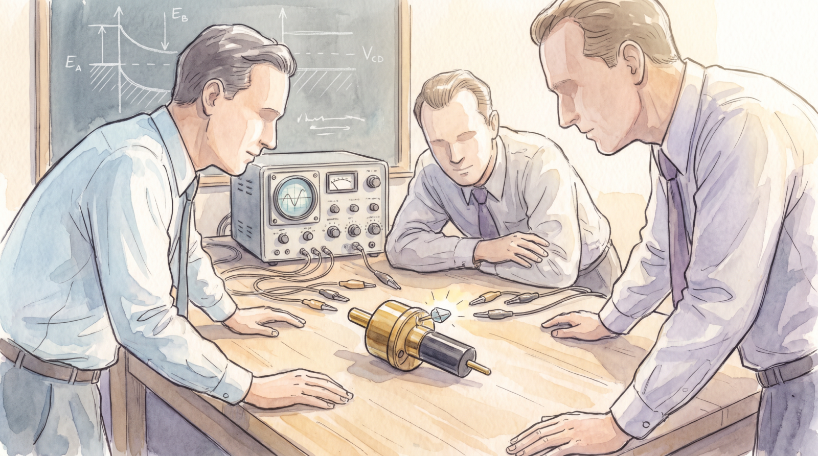
In December 1947, in a sixth-floor laboratory at 463 West Street in Manhattan, two physicists at Bell Telephone Laboratories built a small device out of a strip of gold foil, a tiny piece of germanium, and a bent paper clip. They had been working on the device for about six weeks. The device, when wired to a small source of electric current, did something that a vacuum tube was supposed to do. It amplified a signal. The signal went in weak, and it came out strong. The device used no vacuum, no heated cathode, no glass envelope. It was a small block of solid matter with three wires soldered to it. One of the physicists, Walter Brattain, was later asked what he had said at the moment of the first successful demonstration. He said he did not remember. The other physicist, John Bardeen, said later that the team had known, at the moment, that the thing they had built was important. William Shockley, their supervisor, who had not been in the laboratory on the day of the demonstration, was angry that he had not been in the laboratory on the day of the demonstration, and set out to build a better version of the same thing. The better version, the junction transistor, came five weeks later. The three of them shared the Nobel Prize in Physics in 1956. The device they had built, in two slightly different forms, has been the basic building block of every piece of electronic equipment built since. The mobile phone in your pocket, the laptop on your desk, the satellite in orbit, the microwave in the kitchen, the pacemaker in the chest, the airbag sensor in the steering column, and the digital clock on the oven all use variants of the device that was first demonstrated at 463 West Street in December 1947.
The Vacuum Tube and the Problem of Heat
To understand what the transistor replaced, it helps to understand what came before. The vacuum tube, or thermionic valve, was invented in 1904 by John Ambrose Fleming, an English electrical engineer who had been working on the Edison effect, the phenomenon by which a heated metal filament in a vacuum gives off electrons. Fleming’s first tube, the diode, was a simple device: a heated cathode inside a glass bulb, with a metal plate (the anode) nearby, and a vacuum between them. Electrons flow from the heated cathode to the plate, in one direction only, and the device acts as a rectifier, a one-way valve for electric current. The diode was a useful component, but the more interesting device, the triode, came in 1906 from Lee de Forest, an American inventor who added a third element, a control grid, between the cathode and the plate. A small voltage on the grid could control a much larger current flowing from cathode to plate, and the device could amplify a signal. The triode was the first electronic amplifier, and the first device that could take a weak electrical signal and produce a strong one. It was the workhorse of the radio industry, the telephone industry, the television industry, and the early computer industry, from the 1910s to the 1950s.
The vacuum tube, however, was a problematic device. The cathode had to be heated, typically to a temperature of 800 to 1000 degrees Celsius, and the heating element drew a lot of power. The tubes were bulky. A single triode might be a cylinder 5 to 10 centimetres tall and 2 to 3 centimetres in diameter, and an electronic device of any complexity would need dozens of them. The ENIAC, the first general-purpose electronic computer, completed at the University of Pennsylvania in 1945, used about 18,000 vacuum tubes, weighed 30 tons, drew 150 kilowatts of power, and filled a large room. The tubes were also unreliable. The heated cathode would eventually burn out, and the average lifetime of a power tube in a telephone switching station was about 10,000 hours, or a little over a year of continuous operation. The tubes were also fragile, sensitive to vibration and shock, and prone to internal short circuits. A large computer using thousands of tubes was, in practice, a system in which a tube was always failing, and the operator was always finding the failed tube and replacing it. The cost of maintaining the tubes, in money and in downtime, was the limiting factor on the size and complexity of any electronic system.
The search for an alternative had been going on for a generation. The idea of a solid-state amplifier had been around since the 1920s, when the field-effect transistor, a device that uses an electric field to control the flow of current in a semiconductor, was first proposed. Julius Edgar Lilienfeld, an Austro-Hungarian physicist who had emigrated to the United States, filed a patent for a field-effect device in 1926, and a similar device was patented by the German physicist Oskar Heil in 1934. Neither patent described a working device, and the physics of the surface of the semiconductor, where the field-effect would have to act, was not yet well enough understood to allow the construction of a working amplifier. The physics was, however, beginning to be understood. The band theory of solids, the quantum-mechanical theory of how electrons behave in crystalline materials, had been worked out in the late 1920s and 1930s by Felix Bloch, Alan Wilson, and others, and the band theory explained why some materials were conductors, some were insulators, and some were semiconductors. The semiconductor, the material in the middle, was the one with the interesting band gap, the energy range in which the electron states were forbidden, and the band gap was what made the field effect possible. The gap was a few tenths of an electron volt for germanium, and a little over an electron volt for silicon. The two materials would, in the next twenty years, become the two workhorses of the electronics industry.
The wartime emergency accelerated the work. Radar, the major new weapon of the Second World War, required a fast, low-noise detector of microwave signals, and the crystal detector, a small piece of silicon or germanium with a fine wire touching its surface, was the best available. The crystal detector was a small semiconductor device, and the British and American wartime laboratories had become very good at making them. Bell Labs, in particular, had a wartime group working on the crystal detector, and the group was led by a young theoretician named William Shockley. Shockley, in 1945, proposed a field-effect amplifier based on a slab of silicon. The slab, in his design, would have a thin layer of oxide on the surface, a metal electrode on top of the oxide (the gate), and two electrodes on the bottom (the source and the drain). A voltage on the gate would control the current between the source and the drain, in a way that was, in principle, the solid-state equivalent of the vacuum-tube triode.
Bell Labs and the Solid-State Group
Bell Labs, in the late 1940s, was the largest industrial research laboratory in the world, and it had the resources, the freedom, and the institutional patience to take on a long-term project. Bell Labs was owned by the American Telephone and Telegraph Company, and AT&T’s business depended on the long-distance telephone network. The network, in 1945, was already using vacuum tubes in its amplifiers and switching equipment, and the cost of maintaining the tubes was significant. A solid-state amplifier, if it could be built, would reduce the maintenance cost, increase the reliability, and make possible kinds of equipment that the vacuum tube could not. The economics, in other words, were favourable to the research, and the research was funded out of the long-distance telephone revenue, with no requirement that it produce a commercial product in any particular time frame.
Shockley was put in charge of the new solid-state physics group at Bell Labs in 1945, and he recruited Walter Brattain, an experimentalist who had been working on the crystal detector during the war, and John Bardeen, a theoretical physicist from the University of Illinois who had done fundamental work on the band theory of semiconductors during the war. The three of them, with a small support team, were the core of the group. The group’s mandate was to understand the physics of semiconductor surfaces, and to see whether a solid-state amplifier could be built. The group had access to the very pure germanium and silicon that Bell Labs was producing for the wartime radar programme, and they had the instruments and the technical support that the wartime programme had left behind.
The first year of the group’s work was disappointing. Shockley’s original design, the field-effect device with the oxide layer, did not work. The oxide layer was supposed to insulate the gate from the semiconductor, and the surface of the semiconductor was supposed to be controllable by the field. In practice, the surface was not controllable, and the device was, in fact, an open circuit. The phenomenon that was preventing the device from working was not understood. Bardeen, in 1946, proposed that the surface of the semiconductor was the problem: the surface had electrical charges trapped on it, and the trapped charges were screening the interior of the semiconductor from the field effect. The phenomenon became known as the surface state, and Bardeen’s theory of it was one of the most important results of the group’s work, even before the amplifier was built.
The solution to the problem of the surface state came, in the autumn of 1947, from an experiment by Brattain and a graduate student, Robert Gibney, in which the germanium slab was immersed in an electrolyte, a liquid that could provide a continuous supply of ions to the surface. The electrolyte, in effect, made the surface come to a controlled electrical potential, and the field effect inside the germanium became observable. The experiment worked, and the field effect was real. The next step was to see whether the field effect could be used to make an amplifier, and the next step was to find a way to make the contact to the surface, without the electrolyte, in a way that would let the device be a practical solid-state amplifier.
The Point-Contact Transistor
Brattain and Bardeen, in late November 1947, tried a new design. The germanium slab was left in the open air, and a small drop of electrolyte was placed on its top surface. A metal point, the fine end of a gold wire, was pushed into the drop, and the wire was connected to the input signal. A second metal point, the fine end of a phosphor-bronze wire, was pushed into the germanium surface, very close to the first point, and the wire was connected to the output. The two points, separated by about fifty micrometres on the surface, were the gate and the drain of a primitive field-effect amplifier. The device, when wired to a small source of current and a small input signal, did amplify. The output signal, measured on an oscilloscope, was larger than the input signal. Brattain wrote in his notebook on 16 November 1947 that the device showed “power gain” of about 1.5. It was the first working solid-state amplifier.
The next step was to replace the liquid electrolyte with a solid insulator. Brattain, in a series of experiments in the second half of November, tried a thin layer of oxide on the surface, but the oxide did not adhere well to the germanium, and the device was unstable. The breakthrough came, in early December 1947, from a small change in the design. The two metal points were replaced by a small triangular wedge of plastic, the insulating material used for plastic kitchen wrap in the late 1940s, with a thin gold foil glued to the two lower edges. The plastic wedge was pushed down onto the germanium surface, and the two gold foils, separated by a thin slit cut in the foil with a razor, touched the germanium at two points, about thirty micrometres apart. The plastic wedge held the two points in place, and the slit between them defined the distance. The device was a small, hand-built, fragile thing, the size of a paper clip. It was the first point-contact transistor.
The first successful demonstration of the point-contact transistor was on 16 December 1947, in front of a small group of senior Bell Labs executives. The demonstration showed the device amplifying an audio signal: a microphone input drove the input side of the transistor, and a loudspeaker on the output side reproduced the sound, louder than the microphone alone could produce. The executives, including the president of Bell Labs, were impressed. They were also, characteristically of a corporate research lab, careful to think about the patent implications. The point-contact transistor, in the patent that Bell Labs would eventually file, was credited to Bardeen and Brattain. Shockley, who had been excluded from the laboratory on the day of the demonstration, was credited with the junction transistor, the next major variant, which he had been working on in parallel and which he had filed for patent in early 1948. The three of them were credited, in the Nobel Prize in 1956, with the invention of the transistor.
The point-contact transistor was a delicate device, hard to manufacture, hard to use, and limited in its ability to handle high-frequency signals. It was, however, the first transistor, and the first solid-state amplifier. It was also the device that proved that the field effect could be made to work in a practical device, in air, at room temperature, with no vacuum, no cathode, no glass envelope, and very little power. The device that Bardeen and Brattain built in late 1947 was the direct ancestor of every transistor that has been built since.
The three men at Bell Labs came from very different backgrounds. Shockley, born in London to American parents, raised in Palo Alto, educated at Caltech and MIT, was a confident theoretical physicist in his late thirties when the transistor was invented, and he was the kind of scientist who thought in terms of equations and devices. Brattain, born in China to a father who was a teacher at a mission school, raised in the Pacific Northwest, was an experimentalist in his forties with the hands of a careful machinist and the temperament of a long-term patient observer. Bardeen, the youngest of the three, was a quiet Midwesterner from Madison, Wisconsin, educated at the University of Wisconsin and then at Princeton, with a PhD in mathematical physics, and he was the only one of the three who would win a second Nobel Prize (the first was for the transistor; the second, in 1972, was for the theory of conventional superconductivity, which he did with Leon Cooper and Robert Schrieffer). The three of them were, in many ways, the ideal team for the problem they were working on: a strong theorist with a clear vision, an experimentalist with the right temperament for the difficult and the messy, and a second theorist with the physical insight to solve the surface-state problem that the first theorist had overlooked. The team’s success is one of the most cited examples in the literature of innovation of how a small interdisciplinary team, given adequate time and resources, can produce a result that none of them could have produced alone.
The Junction Transistor and the Industry
Shockley, the theorist, was not in the laboratory on the day of the demonstration, and he set out, almost immediately, to build a better version. His design, the junction transistor, was conceptually different from the point-contact device. The point-contact device used a single slab of germanium with two wires touching it. The junction device used three layers of semiconductor, arranged in a sandwich, with two junctions between the layers. The two outer layers were doped with one type of impurity (n-type, with an excess of electrons), and the middle layer was doped with the other type (p-type, with an excess of holes, the positively charged electron vacancies). The two junctions, in the sandwich, were the emitter and the collector, and the middle layer was the base. A small current at the emitter produced a much larger current at the collector, and the ratio of the two currents was the current gain, the figure of merit for the device.
The junction transistor was announced by Bell Labs in July 1951, and it was the device that made the transistor industry possible. The point-contact device had been too delicate and too noisy for commercial use. The junction device was robust, reliable, and reproducible, and it could be manufactured in batches. Bell Labs, with a stroke of strategic generosity that was characteristic of the post-war industrial research model, licensed the junction transistor to other companies for a small fee. The licence was not exclusive. Any company that wanted to manufacture transistors could do so, for a small royalty, and the technology would be available. The goal was to encourage the rapid development of the new industry, and the goal was successful.
The first commercial transistor products were hearing aids, which appeared in 1952 and 1953, and which used the small size and the low power consumption of the transistor to make possible a hearing aid that could fit in or behind the ear, rather than in a separate box. The next commercial product was the transistor radio, which appeared in 1954 and 1955. The Regency TR-1, the first commercial transistor radio, was made by a small American company, and the Sony TR-55, the first Japanese transistor radio, was made by the Tokyo Telecommunications Engineering Corporation, the company that would become Sony. The transistor radio was a sensation. It was small, it was portable, it ran on a small battery, and it cost, in 1955, about $50, which was a lot of money in 1955, but not a prohibitive lot. The radio transformed the consumer electronics industry, and it transformed the semiconductor industry with it.
The material of the transistor was germanium in the early years, and germanium was the material in which the band gap, the carrier mobilities, and the processing techniques were the best understood. Germanium, however, had a problem: it stopped working as a semiconductor at temperatures above about 90 degrees Celsius, and a device that was meant to work in a piece of electronic equipment, which itself might be in a warm room or a warm car, had to be reliable above that temperature. The solution was silicon, which has a higher band gap, and which works as a semiconductor up to about 150 degrees Celsius. The transition from germanium to silicon was a slow process, completed in the early 1960s, and the silicon transistor was the device that allowed the transistor to be used in military, industrial, and aerospace applications, where the temperature range was wider.
The other major development of the late 1950s was the planar transistor, which was invented by Jean Hoerni, a French-American physicist at the Fairchild Semiconductor Corporation, in 1959. The planar transistor used a thin layer of silicon dioxide on the surface of the silicon, and the metal contacts and the doped regions were all fabricated on the flat top surface. The planar process was reliable, reproducible, and scalable, and it was the basis for the next major development, the integrated circuit. The integrated circuit was invented in 1958 and 1959, by Jack Kilby of Texas Instruments, who built a small circuit on a single piece of germanium, and by Robert Noyce of Fairchild Semiconductor, who built a similar circuit on a single piece of silicon, using the planar process. The integrated circuit put many transistors on a single piece of semiconductor, and the number of transistors on a chip, which Gordon Moore of Fairchild predicted in 1965 would double every year, has been doubling, on a slightly slower schedule, every two years, for the next sixty years. Moore’s law, as it became known, is the basic description of the digital age.
From the Junction Transistor to the Modern World
The transistor, in the seventy-five years since the first point-contact device, has gone from a single hand-built amplifier on a workbench at Bell Labs to a single integrated circuit on a chip the size of a fingernail, with several billion transistors on the chip, and a cost of a small fraction of a cent per transistor. The basic physics has not changed. The transistor, in its modern form, is still a three-terminal device in which a small input current or voltage controls a larger output current, and the device is still made out of a semiconductor, almost always silicon. The processing technology has changed, the manufacturing equipment has changed, the scale has changed, and the applications have changed, but the underlying idea, the field effect in a semiconductor, is the same idea that Bardeen and Brattain demonstrated in late 1947.
The modern semiconductor industry, which is one of the largest industries in the world by revenue, is built on the transistor. The world’s largest semiconductor companies, including Intel, Samsung, TSMC, and SK Hynix, are built on the planar silicon process and on the integrated circuit. The world’s largest markets for semiconductors, including personal computers, mobile phones, data centres, automotive electronics, industrial automation, and military electronics, all depend on the transistor. The world’s largest fabs, which are billion-dollar facilities that manufacture chips on twelve-inch silicon wafers using deep ultraviolet lithography, are the modern equivalent of the small laboratory at 463 West Street. The lab had a single device on a workbench. The fab has billions of devices on a wafer, in a clean room, with automated handling, and a capital cost of a few billion dollars per fab. The progression from one to the other was not inevitable, but it was a consequence of the underlying physics and the underlying economics. The transistor was smaller, cheaper, more reliable, and more efficient than the vacuum tube. The integrated circuit was smaller, cheaper, more reliable, and more efficient than the discrete transistor. The very-large-scale integration was smaller, cheaper, more reliable, and more efficient than the small-scale integration. The progression has continued for seventy-five years, and the next step, the next level of integration, is being worked on now.
The other interesting development has been the slow emergence of new semiconductor materials, in the parts of the electronics industry where silicon cannot do the job. Gallium arsenide and other III-V compound semiconductors have higher electron mobilities than silicon, and they are used in microwave and millimetre-wave applications, including radar and high-frequency communications. Silicon carbide and gallium nitride are wide-bandgap semiconductors, with band gaps of about 3 electron volts, and they are used in power electronics, where the high voltage and high current would destroy a silicon device. Two-dimensional materials, including graphene and the transition metal dichalcogenides, are being explored as possible successors to silicon in some applications, although no two-dimensional material has yet been integrated into a commercial device. The frontier of the field is now in new materials, in new device geometries, and in new integration techniques, including the three-dimensional integration of multiple chips in a single package, and the chiplet architecture, in which a system is built out of multiple smaller chips rather than a single large one. The transistor is still the basic building block. The system around it is changing.
The career of William Shockley, in the years after the transistor, is one of the sadder stories of twentieth-century science. Shockley, who had shared the Nobel Prize in 1956, left Bell Labs in 1955 to found Shockley Semiconductor Laboratory in Mountain View, California, a small company that was meant to develop a new kind of silicon transistor. The company did not succeed commercially, and Shockley, in 1957, was removed from management by his own engineers, who left to found Fairchild Semiconductor. Fairchild became one of the founding companies of what is now Silicon Valley. Shockley, in the late 1960s, became a controversial public figure for his views on intelligence and race, and the controversy effectively ended his scientific career. He died in 1989. Brattain retired from Bell Labs in 1967 and lived quietly in Washington State until his death in 1987. Bardeen stayed at the University of Illinois, where he had been a professor of physics and electrical engineering since 1951, and he remained active in research and teaching until his death in 1991. The three men, who had together built the device that would change the world, ended their lives in three very different ways. The device they had built, however, did not stop changing the world.
The most surprising thing about the transistor, in retrospect, is how long the basic idea has lasted. The point-contact device of 1947 is, in its essence, the same device as the modern CMOS transistor, and the basic idea, that a small input signal can control a larger output signal in a semiconductor, has not been improved upon in any fundamental way. The improvements have been in the materials, the manufacturing, the scale, and the integration, not in the underlying physics. The modern CMOS transistor is a billion times smaller than the point-contact device, a million times cheaper, a thousand times more reliable, and a thousand times faster. The improvement, in other words, has been by a factor of 10 to the 18, across the dimensions of size, cost, reliability, and speed, over seventy-five years. The improvement has been made possible by a combination of better physics, better materials, better manufacturing equipment, and a large amount of money and effort, and the improvement has been one of the most consequential in the history of technology. The transistor, in its modern form, is the workhorse of the digital age, and the digital age is, in turn, the dominant economic and social phenomenon of the twenty-first century. The small device that Brattain and Bardeen built on a workbench in 1947, with a strip of gold foil, a small piece of germanium, and a bent paper clip, is the ancestor of the billions of devices that are now in active service, in every country, in every kind of electronic equipment, in every kind of network, and in every kind of human activity. The small device, in 1947, was a single, fragile, hand-built thing. The millions of devices in your mobile phone are the same device, in the same physics, in the same family tree, made by a process that would not have been imaginable in 1947, and operating in a system that would not have been comprehensible to Brattain, Bardeen, or Shockley. The line runs from one to the other, unbroken.
The line, in fact, runs in both directions. The work that Shockley’s group did in the 1940s drew on the wartime work on the crystal detector, which drew on the earlier work on the band theory of solids, which drew on the development of quantum mechanics in the 1920s. The transistor is a child of the quantum revolution, and the quantum revolution is a child of the early twentieth century’s reckoning with the failure of classical physics. Every modern device, in a sense, is a consequence of a long chain of theoretical work and experimental investigation that goes back to the small group of European physicists who, in the 1920s, worked out the basic rules. The transistor was not an accident. The transistor was the moment when a piece of the new physics, the band theory of solids, became a piece of technology. The moment was seventy-five years ago. The technology is still unfolding.
References
- Transistor — Wikipedia, retrieved 14 October 2026.
- History of the transistor — Wikipedia, retrieved 14 October 2026.
- Point-contact transistor — Wikipedia, retrieved 14 October 2026.
- John Bardeen — Wikipedia, retrieved 14 October 2026.
- Walter Brattain — Wikipedia, retrieved 14 October 2026.
- William Shockley — Wikipedia, retrieved 14 October 2026.
- Bell Labs — Wikipedia, retrieved 14 October 2026.
- Vacuum tube — Wikipedia, retrieved 14 October 2026.
- Triode — Wikipedia, retrieved 14 October 2026.
- Lee de Forest — Wikipedia, retrieved 14 October 2026.
- John Ambrose Fleming — Wikipedia, retrieved 14 October 2026.
- Field-effect transistor — Wikipedia, retrieved 14 October 2026.
- ENIAC — Wikipedia, retrieved 14 October 2026.
- Junction transistor — Wikipedia, retrieved 14 October 2026.
- Moore’s law — Wikipedia, retrieved 14 October 2026.
- Integrated circuit — Wikipedia, retrieved 14 October 2026.
- Jack Kilby — Wikipedia, retrieved 14 October 2026.
- Robert Noyce — Wikipedia, retrieved 14 October 2026.
- Regency TR-1 — Wikipedia, retrieved 14 October 2026.
- Sony TR-55 — Wikipedia, retrieved 14 October 2026.
- Riordan, Michael; Hoddeson, Lillian. Crystal Fire: The Invention of the Transistor and the Birth of the Information Age — W. W. Norton, 1997.
- Planar process — Wikipedia, retrieved 14 October 2026.
- CMOS — Wikipedia, retrieved 14 October 2026.
- Jean Hoerni — Wikipedia, retrieved 14 October 2026.
- Fairchild Semiconductor — Wikipedia, retrieved 14 October 2026.
By Mavis · Reading time: about 22 minutes · Filed in Technology.