The Discovery of Graphene
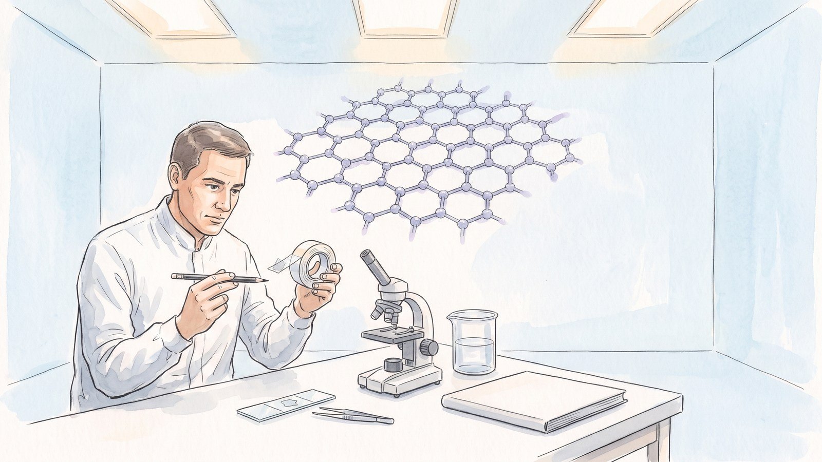
The material that won the 2010 Nobel Prize in Physics was pulled off the end of a pencil with a strip of adhesive tape. There was no machine for it, no clean room, no reactor and no epitaxy chamber. There was a roll of the stuff sold for sealing parcels, a stub of graphite, and two physicists at the University of Manchester who had spent the better part of a decade failing to isolate something that everyone had assumed was impossible to isolate. What they got was a sheet of carbon one atom thick, and the act of peeling it off a piece of ordinary pencil lead turned out to be the first step in a chain of events that ran through the world’s semiconductor industry, earned the Nobel Committee a press release, and left behind a material that is still, more than a decade later, only partly understood.
The Pencil and the Tape
Graphite is old. It was known to the ancients, who found lumps of it in the bedrock around Borrowdale in Cumbria and used it to write on shale; the word comes from the Greek graphites, meaning the thing with which one writes. For most of the twentieth century it was a material with a job rather than a mystery, and the job was done by mixing powdered graphite with kaolin clay and firing the mixture in a kiln. The proportions set the hardness, the hardness set the width of the line, and the invention of the kiln-fired pencil around the 1560s in England is the reason a modern pencil writes at all. Nobody needed to know why graphite worked. It was enough that it did.
What graphite is, physically, took most of a century to establish. The mineral is not pure carbon; it carries silicon and iron impurities, which is why it is a mineral rather than an element. Its structure, worked out through X-ray diffraction in the 1920s and 1930s, is layered. Each layer is a flat hexagonal net of carbon atoms, each bonded to three neighbours in the plane, and the layers are stacked and held to one another by forces far weaker than the covalent bonds within each layer. That difference in strength between the two directions is the whole reason a pencil writes. The layers slide off onto the paper, and they slide off easily, but the bonds holding each layer together are not broken in the process.
The consequences of that layered structure had been industrially useful for a long time before anybody thought to look at it closely. Pure graphite is remarkably soft and it smears, which is why it makes such a good lubricant and why the blades of a steel watch or a lock can be oiled with it; the same weak bonding between the layers lets them slide over one another, which is also why graphite works as a neutron moderator in nuclear reactors, where fast neutrons need to lose energy by bouncing off carbon without being absorbed by it. The pure graphite that came out of the Borrowdale mine in Cumbria in the sixteenth century was so valuable that it was worked as a crown mine, guarded like a state secret, and the theft of it was punishable by death. But it was also too soft and too expensive to use in bulk. The solution, found in the same decade, was to grind it with clay and fire the mixture, which is the entire ancestry of the modern pencil. Clay content set the hardness, hardness set the line width, and the result was a writing implement cheap enough to be universal. The material that would eventually be isolated with adhesive tape had spent four hundred years being turned into a consumable.
The structure itself took until the 1920s to be settled, when the diffraction work of J. D. Bernal and his colleagues established that graphite is built from flat hexagonal sheets of carbon atoms held together weakly, and established that the bonding within a sheet is covalent and directional while the bonding between sheets is not. The same decade brought the recognition that diamond and graphite are the same element in different arrangements, the difference lying entirely in how the bonds are arranged in space rather than in the atoms themselves. What nobody did in the 1920s, or in the sixty years that followed, was seriously consider whether the individual sheet might be isolated.
So the structure of graphite invited an obvious question that nobody had managed to ask usefully for two hundred years. If the layers are held together weakly, and if each layer is a perfect two-dimensional lattice of carbon, then surely one could separate a single layer from the rest. A single layer would be one atom thick. It would be, in the phrase that ended up framing everything that followed, a two-dimensional material, and nobody had ever held one.
The people who finally did were Andre Geim and Konstantin Novoselov, working in Manchester, and the method was almost embarrassingly simple. Press a strip of adhesive tape onto a flake of graphite, peel it away, and the tape comes away carrying part of the flake. Repeat the operation ten or twenty times on the same strip and the material left on it gets thinner each time, as the tape takes away more layers and leaves fewer behind. What Geim and Novoselov had, when they did this, was a piece of graphite with a few dozen layers on it, and they had to work out how many layers any given fragment held.
The way they did that is the part of the story that sounds too clever to be true and is entirely true. They pressed the tape, carrying its fragile cargo of flakes, onto a plate of oxidised silicon, the standard working material of the semiconductor industry. Under an ordinary optical microscope the flakes showed the rainbow interference colours you also see when oil spreads on water. Because the thickness of the silicon dioxide layer beneath them was known to an accuracy of a fraction of a nanometre, the colour of each flake was a direct readout of how thick that flake was. There, under a light microscope in a physics department, were flakes one atom thick. The Nobel Committee’s own popular summary of the prize makes the scale of the achievement plain: a single millimetre of graphite consists of three million layers of graphene stacked on one another.
They published in Science in October 2004, in a paper with the unromantic title Electric Field Effect in Atomically Thin Carbon Films. Geim was fifty-one. Novoselov was thirty-six, and had come to Manchester as Geim’s PhD student from the Netherlands after both of them had started out as physicists in Russia. The laboratory that produced them had a track record of improbable results, including a 1997 experiment that levitated a frog in a magnetic field, which duly won an Ig Nobel prize for being designed to make people laugh first and think second. Seven years before the graphene work, the same group had also worked out how to make adhesive tape that stuck to smooth surfaces like a gecko’s foot. The graphene experiment was not a considered plan so much as the sort of accident that happens in a laboratory with the right habits and enough free time to be wrong.
Believing It
Nobody found it entirely convincing at first, and the reasons were reasonable. The samples were tiny. The evidence for the thickness was optical and indirect. The devices were fragile, and a chemist’s first question is always whether the thing you think you have made is actually a polymer left behind by the transfer process. There was a period, comfortably within the memory of people who worked in the field, when the standard objection was not that the measurements were wrong but that they were too good.
Two things happened in parallel that made the case. The first was that the exfoliation method was so cheap that anybody could try it, and a great many people did. The argument that the samples were polymer-contaminated turned out to have force in a narrower sense than it first appeared, since a genuinely one-atom-thick carbon lattice had never been seen before and there were no established protocols for handling one. The second was the arrival of an entirely different way to make the same thing. Graphene can be grown rather than peeled, by cracking methane over a heated metal surface, and by 2005 the Manchester group and others were producing films of a single carbon layer across areas of square centimetres. Those films were cruder and rougher than a tape-exfoliated flake, and they had to be lifted off the metal and transferred onto an insulating substrate, but they were the same material, and they were made by machinery rather than by hand.
Between those two developments the Manchester group produced the result that convinced the semiconductor industry that something had changed: a room-temperature transistor made from a single carbon layer, reported in Science in 2005, with an on-off ratio in the tens and a carrier density that could be pushed to around a trillion carriers per square centimetre. A transistor with an on-off ratio of thirty was poor by the standards of a machine in which the ratio was routinely a million. But it was being switched with a field-effect device only one atom thick, and the fact that it worked at all meant that the band structure implied by the optical measurements was real, and that it could carry current.
What settled it, in the end, was a combination of the obviousness of the method and the arrival of a completely independent way of making the same thing. Because the exfoliation route required nothing but tape and patience, it was reproduced in laboratories all over the world within months. At the same time, other groups were growing graphene from methane on heated nickel or silicon carbide, and those films, though cruder and less uniform, gave the same answer when measured. Two entirely different routes converging on the same material is what turned a curiosity into a fact.
The decisive evidence, though, was electrical. A flake of graphene deposited on the oxidised silicon sat on top of an insulator with a conducting plate underneath, which makes a capacitor with a gap of a fraction of a nanometre. Apply a voltage between the flake and the silicon and you push charge into the graphene or pull it out, and the resistance of the flake responds. That is the field effect, and in 2004 the Manchester group reported it in single layers, with carrier densities reaching around a trillion carriers per square centimetre and a device that could be switched between conducting and not conducting. A transistor made from a layer one atom thick, in which the number of atoms carrying the current was the number of atoms in the flake. The on-off ratio was unimpressive by the standards of the silicon transistors of the day, a matter of tens rather than millions, but the transistors were being made from a sheet with no thickness at all.
By 2005 the group had the direct images that the optical method implied, showing the hexagonal lattice, and had made the thing that would eventually look most like proof to the public: a quantum Hall effect in graphene, measured at room temperature and with the unmistakable signature of massless particles. In October 2010 the Royal Swedish Academy of Sciences awarded the Nobel Prize in Physics jointly to Geim and Novoselov “for groundbreaking experiments regarding the two-dimensional material graphene”. The announcement was made on a Tuesday afternoon, and the Academy’s popular information sheet opened with the observation that a thin flake of ordinary carbon, one atom thick, lies behind the year’s prize.
The popular sheet also made the point that the Nobel Committee thought worth making explicitly, and it is the right way to end the story of the discovery itself. Both laureates, it noted, think research should be fun; they allowed themselves to be led through the labyrinths of chance, and had the luck and the knowledge to seize on opportunities as they appeared, as we all know chance favours only the prepared mind. The graphene work was the outcome of a decade of playing with materials in a laboratory that had spent the decade after the frog learning how to make tape that stuck to things, and of a willingness to try something that everybody knew was impossible.
What the Material Does
The reason graphene mattered was never any single property. It was that it combined several extraordinary properties in the same object, and that almost none of them can coexist in any other material known to materials science.
It conducts electricity as well as copper, and it carries heat better than any other known material. It is almost completely transparent, absorbing only a small fraction of the light that falls on it, and it is so dense that not even helium, the smallest gas atom, can pass through a sheet of it without difficulty. Its tensile strength makes it the strongest material ever measured, and the stiffness of the lattice is such that a graphene ribbon could be stretched by about ten per cent before breaking, which is extraordinary for something in the strength class of diamond. The Nobel Committee’s popular information sheet put the summary bluntly: graphene is not only the thinnest material ever made but also the strongest, it performs as well as copper as a conductor of electricity, it outperforms all other known materials as a conductor of heat, and it is almost completely transparent while being dense enough that not even helium can pass through it.
Those are extraordinary in combination rather than individually. Copper conducts superbly and is useless as a transparent window. Diamond is hard and thermally excellent and cannot be rolled out into a sheet a single atom thick. The point of graphene is that it takes the properties that in other materials are mutually exclusive and puts them all in the same plane, which is a way of saying that it has almost no bulk and almost no internal structure to get in the way.
The strength was measured directly in 2008, when a group at Columbia suspended flakes of graphene over holes in a substrate and pulled them with the tip of an atomic force microscope until they broke. The intrinsic strength that came out, of the order of a hundred times that of steel, and a stiffness in the region of a terapascal, are properties of the perfect lattice rather than of the samples tested, since the measured values are limited by defects and by the size of the flake. It is a standard result in the field, and a slightly deflating one, that a graphene ribbon is nearly always stronger than any comparable specimen of anything else and yet is usually weaker than its own theoretical value, because the sample is never as good as the material.
The same flatness that makes the lattice strong gives graphene a surface area that is startling when you do the arithmetic. One gram of graphene, if it could be separated into single layers, would present roughly thirteen hundred square metres of surface. That figure is why the material is of interest to people thinking about catalysis, filtration and membranes, where area is what matters, and it is also why graphene looks, on paper, like a solution to a very large number of problems at once. It is worth holding on to the fact that this is a consequence of the geometry rather than a special property: any material made of one-atom-thick sheets would have the same area, and very few of them would survive being isolated.
Two of the measurements are worth knowing precisely, because they are the ones that were contested and revised. The transparency was settled in 2008 by Nair and colleagues at Manchester, who measured a single layer and found that it transmits about 97.7 per cent of visible light, absorbing the remaining 2.3 per cent. The remarkable part was not the number but its exactness: the absorbed fraction is set by the fine structure constant, the fundamental constant that sets the strength of electromagnetism, so the optical behaviour of a one-atom-thick layer of carbon is as close to a fixed number of nature as anything measured in a materials laboratory.
The thermal conductivity took longer and was revised more than once. Measurements on a suspended single layer, published by Balandin and colleagues in 2008 in Nano Letters, gave a figure in the thousands of watts per metre per kelvin, several times that of copper and far above diamond. The number has been argued over since, partly because later samples were cleaner than the first ones and partly because heat conductance in a two-dimensional body is not the same quantity as heat conductivity in a bulk solid, and the comparison with a three-dimensional material can be misleading. What nobody disputes is the order of magnitude, and that a single layer of carbon carries heat better than anything else known.
The strength came from the geometry itself. Each carbon atom in the lattice has three strong bonds to its neighbours and the fourth electron sits in a p orbital above and below the plane. The bonds are directional, which is why the sheet is stiff rather than floppy, and the absence of any bulk means that there are no grain boundaries or defects of the kind that limit a metal. A perfect graphene ribbon should be the strongest material in existence; what is measured is what survives the growth process.
The Physics of Two Valleys
What makes graphene interesting to physicists is not only that it is thin but that being thin changes the mathematics. When an electron moves in the graphene lattice, it does not behave like an electron in a conventional semiconductor. It does not have an effective mass in the usual sense, and it does not obey the ordinary Schrodinger equation. At low energies its motion is described by the Dirac equation, the same equation that governs a relativistic particle, with the speed of light replaced by a Fermi velocity of roughly one three-hundredth of the speed of light. Electrons in graphene behave like massless particles with an unusual dispersion relation, and the system turned out to be a laboratory for ideas first developed for relativistic field theory.
The lattice itself has a symmetry that produces the effect. The honeycomb net has two inequivalent sets of corners, usually called the valleys, and an electron’s wavefunction picks up a phase of pi when it is carried round a closed loop in the lattice. That phase, the Berry phase, is what produces the most striking experimental result in the whole story. In 2007 the Manchester group reported the quantum Hall effect in graphene, and it was not the integer version that everyone else was used to. The Hall conductance did not climb in steps of one, two, three. It climbed in steps of two, six, ten, in units of the conductance quantum, the pattern that would be expected from massless particles carrying half-integer charge, and it did so at room temperature and in a device that could be handled with tweezers. It is a quantum Hall effect with half-integer steps, a signature that had been predicted for other systems for two decades and could not be observed in any of them.
The geometry behind this is worth spelling out, because it is unusual and because everything else follows from it. The hexagonal net has two kinds of corner, and they are not equivalent: in the language of the band structure, the electronic bands touch at two points of the Brillouin zone, called the valleys, which sit at the corners of the hexagonal zone and are related to one another by a reflection rather than by a rotation of the lattice. Halfway between two of those points the bands are furthest apart, which is where the group velocity vanishes and the electrons are effectively stationary. The Berry phase of pi is a consequence of the way the wavefunction is forced to realign as it is carried around the loop of the lattice, and it is that phase, not the geometry alone, which fixes the half-integer steps in the Hall conductivity.
The energy levels in a magnetic field make the same point in a different register. In an ordinary two-dimensional electron gas the levels are equally spaced and the Hall conductance climbs in units of the conductance quantum. In graphene the levels are spaced like the square root of the magnetic field, the lowest level sits at zero energy and is half filled, and the conductance climbs in steps of two, six, ten. The half-integer sequence is the signature of the Dirac spectrum, and finding it in a material made by peeling graphite onto a piece of oxidised silicon was, in 2007, one of the most striking single results in the history of condensed matter physics.
Graphene also made sense of the rest of carbon. The nanotubes discovered in 1991 were made by rolling up cylinders of graphene, and the possibility of that was implicit in the sheet itself; in 2008 Harutyunyan and Yakobson showed computationally that a graphene sheet could simply be rolled up, and the graphene scroll was recognised as a natural precursor of the nanotube. The same lattice also produces the vibrational signature that made graphene easy to identify: the two characteristic Raman bands, the G band and the 2D band, the second of which shifted with the number of layers and so provided a quick way to count them. The material turned out to explain a family of things rather than to be an entirely new one, which is one of the reasons it spread so fast through the literature.
There is one further structural feature worth noting, because it is the reason graphene behaves so differently from ordinary materials in three dimensions. A sheet can bend, and the bending of a two-dimensional body produces a vibrational mode with a quadratic rather than linear dispersion, unlike every ordinary solid. These out-of-plane modes, the flexural phonons, are unusually soft and unusually long-lived, and they alter how heat is carried in the plane and how electrons scatter. A great deal of the theoretical interest in graphene since 2004 has been in this direction, and it remains an active subject rather than a closed one.
The Long Road to a Device
Six years after the discovery, the thing that stood between graphene and any application was not fabrication but physics. A transistor needs to be switched off as well as on, and the mechanism for switching it off is a band gap: an energy range that no electron can occupy, so that a barrier cannot be crossed. Graphene has no band gap. Its conduction and valence bands meet at a single point, and an electron arriving at a potential barrier tunnels straight through it. A graphene transistor therefore conducts whether or not you apply a voltage to it, which means the off state leaks and the on-off ratio is useless. The Nobel Committee’s own summary of the prize put the difficulty plainly: graphene’s transistors are predicted to be substantially faster than silicon ones, and silicon has already reached the size at which the material stops working properly, so graphene’s limit should be lower still. But a lower limit on size is useless if the switch cannot be turned off.
The proposed answers all involved making the sheet less perfect. A ribbon a few nanometres wide, made by cutting a graphene sheet, has edges that confine the electrons and open a gap. Stacking two sheets and applying a field across them opens a gap too, without needing edges at all. Stretching the lattice distorts the bands. Chemically modifying the carbon changes what the electrons can do. None of these is elegant, and each costs something: a narrow ribbon carries less current, a bilayer device is harder to make, and both are harder to produce reliably over large areas. The best of the early results, reported in Nature Nanotechnology in 2010, produced graphene nanoribbon transistors with on-off ratios of a hundred thousand and more, which was enough to be a device rather than a curiosity, but only at low temperature, and with current levels far below what a practical circuit would need.
It is worth being precise about why the absence of a gap is not merely a defect of the material but a restatement of its advantage. Silicon, which has an indirect gap of roughly one electronvolt, cannot be made into a perfect switch either; the leakage that results is exactly what has limited the industry for four decades and driven it towards ever smaller transistors and ever more elaborate gate structures. Graphene has no gap at all, which means the same absence that makes it useless as a switch also makes it the best conductor ever measured in a laboratory, because its electrons have nothing to scatter from. The single missing quantity is the one that a transistor needs and a wire does not, and the entire effort of the field has been directed at adding it back without destroying everything else.
That effort has produced a large literature and a large infrastructure. The field acquired its own quality-control conventions, its own characterisation standards, and eventually its own shared vocabulary for the ways in which a sample can be wrong: polymer residue, wrinkles, ripples, edges, substrate strain, and the slow drift of a material that adsorbs whatever is in the air around it. Some of this was a necessary correction of work that had been published on the assumption that a perfect lattice was what was under the microscope.
There was a second problem, and it was more embarrassing. The method that discovered graphene was a laboratory method: a piece of tape, one flake at a time, a microscope, and an enormous amount of patience. It could never produce a material in quantity. The route that could was growth, depositing carbon vapour onto hot metal, and by the middle of the 2010s chemical vapour deposition on copper foil was producing continuous graphene films measured in centimetres. But growth produces a film that has to be lifted off the copper and put somewhere else, and the standard way of doing that involved coating it with a polymer, which leaves a residue. And then the uncomfortable finding: a good deal of what had been measured as graphene’s properties in the early years was in fact the polymer. Raman spectroscopy became the field’s screening tool, the way a quality-control department tests incoming material, and a great deal of published work had to be repeated.
By 2012 the community was writing its own account of what needed to happen next. The roadmap for graphene, published in Nature that year by a wide group of authors from eighteen countries, set out the material science, the characterisation standards and the manufacturing questions that stood between the laboratory and a product. It is a document worth reading for a more general reason, because it reads like a field admitting that it has a physics problem and a chemistry problem before it has an engineering problem.
The money that followed was unprecedented for a single material. The European Union’s Graphene Flagship, launched in October 2013 and coordinated from Chalmers University in Gothenburg, was the largest research programme the Union had ever funded, on the order of a billion euros spread across ten years and dozens of institutions, with a graphene engineering innovation centre built in Manchester to attack the manufacturing side. Manchester had already established a graphene engineering innovation centre of its own. Other large national programmes followed, and the term that settled into general use for the material’s status was the one from the title of the 2004 paper: two-dimensional material.
So far the honest verdict is that graphene has not replaced silicon, and the early predictions of transparent displays and bendable phones have not arrived. Its real uses have been smaller and stranger: conductive inks and coatings, thermal management films, the reinforcement of composites, and above all the research platform, where graphene has become the standard system for studying condensed matter because its band structure is known exactly and can be tuned by applying a voltage. That is a considerable understatement of what it did. The Nobel Prize was not awarded for a better transistor. It was awarded for the demonstration that a genuinely two-dimensional material can exist and can be handled in a laboratory by people with ordinary equipment, which is the kind of result that changes what a field believes is possible rather than what it can ship.
And the method that did it is still the method. The tape, the graphite, the oxidised silicon plate, the optical microscope. More than two decades after the paper, the fastest way to obtain graphene remains the one that a postdoctoral fellow can carry out at a bench with a pencil and a roll of parcel tape, and the reason so much of the field’s most interesting physics was done so quickly is that the material was available to anyone with an afternoon and an idea. That, in the end, is the part of the story that has aged best.
References
- The Nobel Prize in Physics 2010 - The Royal Swedish Academy of Sciences, 5 October 2010
- Graphene - the perfect atomic lattice - The Royal Swedish Academy of Sciences, popular information, 2010
- The Nobel Prize in Physics 2010 - press release - The Royal Swedish Academy of Sciences, 5 October 2010
- The Nobel Prize in Physics 2010 - advanced information - The Royal Swedish Academy of Sciences, 2010
- Andre Geim - facts - NobelPrize.org, 2010
- Konstantin Novoselov - facts - NobelPrize.org, 2010
- Electric Field Effect in Atomically Thin Carbon Films - K. S. Novoselov, A. K. Geim, S. V. Morozov, D. Jiang, Y. Zhang, S. V. Dubonos, I. V. Grigorieva and A. S. Firsov, Science 306, 666-669, 2004
- Two-Dimensional Atomic Crystals - K. S. Novoselov, D. Jiang, F. Schedin, T. J. Booth, V. V. Khotkevich, S. M. Morozov and A. K. Geim, Proceedings of the National Academy of Sciences 102, 10451-10453, 2005
- The rise of graphene - A. K. Geim and K. S. Novoselov, Nature Materials 6, 183-191, 2007
- Room-Temperature Quantum Hall Effect in Graphene - K. S. Novoselov, D. Jiang, Y. Zhang, S. V. Morozov, S. V. Dubonos, I. V. Grigorieva and A. K. Geim, Science 315, 1379-1382, 2007
- Fine Structure Constant Defines Visual Transparency of Graphene - R. R. Nair, P. Blake, A. Grigorenko, K. S. Novoselov and A. K. Geim, Science 320, 1308, 2008
- Superior Thermal Conductivity of Single-Layer Graphene - A. A. Balandin, S. Ghosh, H. Bao, Z. Tian, X. Cui and M. Calizo, Nano Letters 8, 902-907, 2008
- Measurement of the Elastic Properties and Intrinsic Strength of Monolayer Graphene - C. Lee, X. Wei, J. W. Kysar and J. Hone, Science 321, 385-388, 2008
- Graphene transistors - K. Klein, J. Zhao, A. Kh. Shukir, D. A. Kitchin, A. P. Thompson, D. Anderson, H. S. Shen, S. M. Bayer, J. E. Fromm, L. A. Sizes, E. J. Lipson and A. K. Geim, Nature Nanotechnology 5, 827-831, 2010
- A roadmap for graphene - K. S. Novoselov, V. I. Falko, S. Colombo, F. Schedin, A. K. Meyer and others, Nature 490, 192-200, 2012
- Graphene Flagship - Graphene Flagship, European Commission research programme
- The Home of Graphene - University of Manchester
- October 22, 2004: Discovery of Graphene - APS News, October 2009
- Graphene - Wikipedia
- Andre Geim - Wikipedia
- Konstantin Novoselov - Wikipedia