The Monolithic Giant – Wafer-Scale Silicon
The Monolithic Giant – Wafer-Scale Silicon
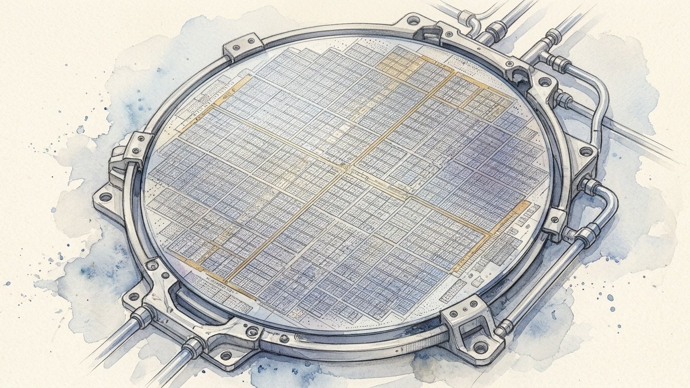
For more than six decades, the foundational manufacturing ritual of the global semiconductor industry has followed an invariant, unyielding script: grow an ultra-pure cylindrical monocrystalline ingot of electronic-grade silicon, slice it into round 300-millimeter circular wafers polished to atomic flatness, print hundreds of identical microscopic integrated circuits onto the surface using deep ultraviolet photolithography, and then immediately take a high-speed diamond-bladed saw and cut the wafer into hundreds of tiny individual rectangular microchips. In the era of modern artificial intelligence, where deep neural networks with hundreds of billions of parameters require distributed clusters of thousands of GPUs tied together with fragile copper and optical cables, this traditional dicing ritual represents a catastrophic architectural tax: the moment a chip is sliced from the wafer, its communication bandwidth with neighboring silicon drops by a factor of ten thousand, while latency surges by a factor of one thousand. In 2019, a audacious Silicon Valley startup named Cerebras Systems shattered this sixty-year manufacturing dogma by posing a radical, seemingly insane question: What if we don’t cut the wafer? The creation of the Wafer Scale Engine (WSE)—culminating in the WSE-3, a monolithic slab of continuous silicon measuring 46,225 square millimeters containing four trillion transistors and 900,000 AI-optimized cores on a single unbroken plate—stands as one of the supreme mechanical, thermal, and microarchitectural engineering triumphs in the history of technology, conquering the five historic impossibilities of wafer-scale computing and fundamentally redefining the physical boundaries of compute.
1. The Sacred Ritual – Slicing the Silicon Wafer
To appreciate the sheer audacity of wafer-scale computing, one must understand the economic and physical imperatives that established the traditional semiconductor manufacturing paradigm. In a state-of-the-art semiconductor fabrication facility (a ‘fab’)—such as TSMC’s GigaFabs in Hsinchu or Tainan—silicon manufacturing begins with a circular disk of pure monocrystalline silicon measuring 300 millimeters (approximately 12 inches) in diameter and roughly 775 micrometers in thickness.
This pristine disk represents the most perfect crystalline substrate manufactured by human civilization: fewer than one in a billion atoms is an unwanted impurity. Onto this wafer, extreme ultraviolet (EUV) photolithography steppers project complex circuit patterns layer by layer, utilizing 13.5-nanometer light reflected through multi-layer molybdenum-silicon mirrors to pattern billions of microscopic transistors, finFETs, and nanosheets across dozens of lithographic mask layers.
Yet, the physical optics of photolithography steppers impose a hard geometric limit: The Reticle Limit. An EUV photolithographic scanner cannot expose an entire 300 mm wafer in a single flash of light. The optical field of the scanner lens is constrained to a maximum rectangular exposure area of approximately 26 millimeters by 33 millimeters—a maximum die area of roughly 858 square millimeters. To pattern an entire wafer, the stepper must step across the surface in a grid-like fashion, flashing the reticle pattern dozens of times, leaving narrow unpatterned borders between adjacent exposure fields known as ‘scribe lines’ or ‘dicing streets.’
Once fabrication is complete, the wafer is delivered to a dicing saw. High-speed diamond saws spinning at 60,000 RPM slice along the scribe lines, dicing the wafer into hundreds of isolated microchips. Each tiny die is picked up, mounted onto a fiberglass substrate, sealed in plastic or ceramic packaging with solder ball arrays (BGA), and soldered onto a printed circuit board. For sixty years, this dicing ritual was universally accepted as an unavoidable physical law of nature.
2. The Tyranny of the Die Boundary – The Off-Chip Bandwidth Chasm
While dicing wafers made sense in the era of single-core microprocessors and personal computers, in the era of modern artificial intelligence and frontier scientific computing, the physical boundary of the microchip has become a crippling bottleneck. Deep learning is an intrinsically distributed computational problem: training a modern multi-hundred-billion-parameter Transformer requires tens of thousands of individual GPUs operating in tight, synchronized coordination.
The moment an electron attempts to cross the boundary from one silicon chip to another, it encounters a catastrophic physical chasm: – On-Chip Interconnects: Inside a single silicon die, microscopic copper interconnect wires measure mere tens of nanometers in width and run for a few micrometers. Moving a 64-bit word across on-chip wires consumes less than 0.1 picojoules of energy and takes fractions of a nanosecond, operating with aggregate internal memory bandwidths exceeding tens of terabytes per second. – Off-Chip Interconnects: To move that same 64-bit word off the chip, the signal must travel through on-chip I/O drivers, cross a micro-bump, navigate a silicon interposer or packaging trace, cross a solder ball onto a printed circuit board, travel through a copper PCB trace, pass through a PCIe connector, enter a network interface card (NIC), convert into optical photons via a laser transceiver, travel through an optical fiber, and reverse this entire gauntlet at the destination chip!
This off-chip journey consumes between 10 to 30 picojoules per bit—hundreds of times more electrical power than the calculation itself! Furthermore, physical pin counts and wire routing bottlenecks restrict the total bandwidth: an advanced GPU (such as an NVIDIA H100) possesses an on-chip SRAM bandwidth of approximately 33 terabytes per second, but its off-chip NVLink communication bandwidth is capped at 900 gigabytes per second—a forty-fold collapse in bandwidth the instant data leaves the silicon die. Thousands of expensive GPUs spend massive fractions of their operational time stalled, waiting for network packets to cross external cables. The dream of computer architecture has always been obvious: eliminate the off-chip boundary entirely by turning the entire wafer into a single, continuous, monolithic superchip.
3. The Ghost of Gene Amdahl – The Trilogy Systems Tragedy
The concept of Wafer-Scale Integration (WSI) was not new. In the early 1980s, one of the greatest legends of computer architecture—Gene Amdahl, the chief architect of the IBM System/360 mainframe and formulator of Amdahl’s Law—set out to commercialize wafer-scale integration by founding Trilogy Systems in Silicon Valley.
Amdahl recognized the immense speed advantages of keeping signals on a single wafer. Backed by hundreds of millions of dollars in venture capital and corporate investment (the largest venture-backed startup in history at that time), Trilogy attempted to build a 2.5-inch ECL (Emitter-Coupled Logic) wafer-scale mainframe processor. The project ended in a historic, catastrophic failure. In 1984, Trilogy collapsed after burning through $300 million without ever delivering a working commercial computer. The failure was so spectacular that for the next thirty-five years, ‘wafer-scale integration’ became a taboo phrase in semiconductor venture capital—a concept widely derided as an engineering graveyard.
Trilogy failed because it collided with two unforgiving physical and statistical laws that seemed insurmountable with twentieth-century technology:
1. Murphy’s Yield Law and Defect Probability
In semiconductor manufacturing, no silicon wafer is ever 100% perfect. Airborne dust particles, crystalline imperfections in the silicon substrate, and chemical resist residue introduce microscopic physical defects across the wafer. The yieldY(the percentage of functional chips) follows the classic Poisson or Murphy defect model:
In traditional semiconductor manufacturing, wafer yield obeys an unforgiving exponential law: as the surface area of a chip grows, the probability of containing fatal microscopic defects increases exponentially. Because silicon wafers invariably contain a baseline density of crystal dislocations and dust particles, attempting to fabricate an unbroken die larger than a few square centimeters typically results in near-zero yield.
whereAis the area of the chip andDis the defect density (defects per square centimeter). For a tiny chip of 100 mm², yield can exceed 90%. But as chip areaAexpands, defect probability grows exponentially. For a wafer of 46,000 square millimeters, the probability of obtaining a completely defect-free wafer is mathematically equivalent to zero. A single microscopic short-circuit on a power plane would brick the entire multi-million-dollar wafer.
2. The Thermal Expansion Disaster
When an operating computer processor heats up, it physically expands. Monocrystalline silicon has a low coefficient of thermal expansion (roughly 2.6 parts per million per Kelvin). Standard printed circuit board materials (such as FR4 fiberglass) expand at roughly 14 parts per million per Kelvin—more than five times faster! In a tiny 20 mm chip, this expansion differential is negligible. But across a 300 mm wafer, the edge of the circuit board expands by hundreds of micrometers relative to the silicon, generating catastrophic mechanical shear stresses that rip solder balls off the pads and shatter the brittle silicon wafer like a pane of glass.
4. The Audacious Gamblers – Andrew Feldman, Sean Lie, and the Genesis of Cerebras
In 2015, serial entrepreneur Andrew Feldman, hardware architect Sean Lie, and systems engineer Gary Lauterbach gathered in Los Altos, California, to plan their next venture. They had previously founded SeaMicro, pioneering micro-server architectures before selling the company to AMD for334 million. Looking at the meteoric rise of deep learning, they recognized that the deep neural networks of the future would require millions of cores and petabytes of bandwidth that traditional GPU clusters could never deliver efficiently.
Sean Lie proposed the unthinkable: it was time to resurrect wafer-scale integration. Lie argued that the three-decade-old failure of Trilogy Systems had occurred because semiconductor manufacturing, material science, and packaging were primitive in 1980. In 2016, modern foundries like TSMC possessed defect densities so low, lithographic alignment so precise, and automated packaging so advanced that the five historic ‘impossibilities’ of wafer-scale computing could finally be conquered by modern engineering.
In 2016, they founded Cerebras Systems. Over the next three years, working in absolute secrecy and partnering closely with Taiwan Semiconductor Manufacturing Company (TSMC), Cerebras systematically dismantled every physical, mechanical, thermal, and algorithmic barrier that had doomed previous generations of engineers.
5. Conquering the First Impossibility – Cross-Reticle Stitching
The first physical barrier was the reticle limit of photolithography steppers. A TSMC scanner can only expose an 858-square-millimeter field. On a standard wafer, the scribe lines between reticle fields are waste zones reserved for test structures and dicing saws; no electrical wires ever cross from one reticle field to another.
To create a continuous, monolithic processor across an entire 300 mm wafer, Cerebras and TSMC had to invent Cross-Reticle Lithographic Stitching. Working at TSMC’s advanced fab facilities, the engineers modified the photolithographic masking process. Instead of leaving dead dicing streets, they engineered specialized lithography masks that overlap precisely across the reticle boundaries.
In the upper metal interconnect layers of the wafer (where copper wires are thicker and more robust), lithography steppers print continuous microscopic copper interconnects that traverse directly across the scribe lines, stitching the 84 individual reticle fields together into an unbroken, seamless 2D communication mesh. When electrons travel across the stitched boundary from Reticle 42 to Reticle 43, they travel through continuous copper wires at silicon speed, experiencing zero impedance mismatch, zero capacitive packaging penalties, and zero latency drop. The entire wafer became an electrically unified, single sheet of silicon.
6. Conquering the Second Impossibility – Hardware Redundancy and 100% Yield
The second impossibility was Murphy’s Yield Law. Even in TSMC’s ultra-clean 16-nm, 7-nm, and 5-nm cleanrooms, a 300 mm wafer will inevitably contain hundreds of microscopic physical defects—particulate dust, crystal dislocations, or gate dielectric breakdowns. If Cerebras required every single transistor on the wafer to be perfect, their commercial yield would be 0%.
Sean Lie and the Cerebras architecture team conquered this through an elegant mathematical strategy: Fine-Grained Hardware Redundancy and Dynamic Re-Routing.
Instead of building giant, monolithic processing cores, Cerebras designed the Wafer Scale Engine around hundreds of thousands of tiny, identical, independent processing cores (tiles). Built into the silicon fabric is an extra 1.5% to 2% of redundant spare cores distributed evenly across the wafer, alongside redundant communication channels in the 2D mesh.
During initial factory testing, automated wafer-probing diagnostics map every single defect on the wafer with micron precision. If a particle defect destroys Core #512 in Row 84, the hardware does not discard the wafer. Instead, on-chip electronic configuration registers permanently disconnect the dead core and dynamically slide the logical coordinate system over by one position, activating a neighboring redundant core. The 2D mesh communication fabric simply routes data around the dead node with zero software intervention. Through this self-healing architectural redundancy, Cerebras transformed an impossibly fragile, 46,000-square-millimeter silicon monster into a robust commercial product that achieves 100% functional wafer yield!
7. Conquering the Third Impossibility – The Thermal Expansion Elastomer
The third impossibility was the catastrophic thermal expansion mismatch between silicon and printed circuit board materials. If a 300 mm wafer is soldered rigidly to a motherboard, the differential expansion during thermal cycling will shatter the wafer or tear the electrical contacts off the package.
Cerebras discarded standard solder balls and rigid packaging entirely, inventing a revolutionary mechanical and materials stack: 1. The Custom Elastomeric Spring-Pin Interface: Instead of soldering, the wafer is connected to the external world through a massive array of thousands of microscopic, flexible elastomeric spring-pins (pogo-pins) that contact gold-plated pads on the back of the wafer. These micro-springs can compress and flex laterally by hundreds of micrometers, maintaining continuous electrical contact while allowing the silicon wafer and the circuit board to expand and contract completely independently at different rates without mechanical stress. 2. The Intermediate Expansion Alignment Plate: Cerebras engineered an intermediate mechanical carrier plate fabricated from a specialized metal alloy with a coefficient of thermal expansion precisely matched to that of monocrystalline silicon. This plate holds the brittle wafer under perfectly calibrated mechanical tension, preventing warping, bowing, or micro-cracking across temperature excursions from 20°C to 100°C.
8. Conquering the Fourth and Fifth Impossibilities – 23 Kilowatts of Power and Water Cooling
The final two impossibilities were the twin titans of thermodynamics: Power Delivery and Heat Dissipation.
Delivering 30,000 Amperes of Direct Current
A flagship Cerebras Wafer Scale Engine consumes approximately 23,000 watts (23 kilowatts) of electrical power. At an operating voltage of roughly 0.8 volts, this requires delivering an unimaginable current of nearly 30,000 amperes to the wafer!
In a standard chip, power is routed laterally through the edges of the package. If you attempted to feed 30,000 amperes laterally through the edges of a 300 mm wafer, the immense electrical resistance across the thin copper traces would cause massive resistive I² R heating: the edges of the wafer would melt, and voltage at the center would drop to zero (the IR drop catastrophe). Cerebras solved this by engineering Perpendicular Vertical Power Delivery. Power is brought in perpendicularly through the back of the wafer: thousands of custom current-carrying power distribution pins feed power directly into the local silicon tiles across the entire 2D surface, minimizing resistive loss and maintaining an ultra-stable, uniform 0.8-volt supply across every square millimeter of the wafer.
Direct-Contact Closed-Loop Water Cooling
Dissipating 23 kilowatts of concentrated heat from a thin, brittle plate of silicon smaller than a dinner plate is an unprecedented thermal challenge. Air cooling was physically impossible: air lacks the thermal heat capacity to cool such power density. Placing a standard copper water block against the wafer would crush the brittle silicon under mechanical clamping pressure.
Cerebras engineered a custom, direct-contact Laser-Cut Cold Plate. The cold plate is mounted directly against the wafer, separated only by a micron-thin layer of high-performance thermal interface material. Inside the plate, a dense network of thousands of microscopic, laser-machined channels circulates chilled water at high flow rates under uniform hydrostatic pressure. The fluid dynamics are designed to prevent localized hotspots, ensuring that every single one of the 900,000 cores operates at a stable, uniform temperature, extracting 23 kilowatts of thermal energy silently and continuously.
9. The Architectural Masterpiece – WSE-1, WSE-2, and WSE-3
Between 2019 and 2024, Cerebras demonstrated that wafer-scale computing was not a one-off engineering fluke, but an aggressive, repeatable scaling roadmap spanning three successive semiconductor process generations:
| Specification | Cerebras WSE-1 (2019) | Cerebras WSE-2 (2021) | Cerebras WSE-3 (2024) |
|---|---|---|---|
| Foundry Process | TSMC 16-nanometer | TSMC 7-nanometer | TSMC 5-nanometer |
| Silicon Die Area | 46,225 mm² | 46,225 mm² | 46,225 mm² |
| Transistor Count | 1.2 Trillion | 2.6 Trillion | 4.0 Trillion |
| AI Compute Cores | 400,000 cores | 850,000 cores | 900,000 cores |
| On-Chip SRAM Memory | 18 Gigabytes | 40 Gigabytes | 44 Gigabytes |
| Memory Bandwidth | 9 Petabytes / second | 20 Petabytes / second | 21 Petabytes / second |
| Fabric Bandwidth | 100 Petabits / second | 220 Petabits / second | 214 Petabits / second |
| Peak AI Performance | — | — | 125 PetaFLOPs (FP16) |
To contextualize these numbers: the WSE-3 contains 56 times more silicon area than the largest single GPU ever manufactured by NVIDIA (the H100, which measures 814 mm²). Its 44 gigabytes of on-chip SRAM provides an aggregate memory bandwidth of 21 Petabytes per second—more than six thousand times greater than the HBM3 memory bandwidth of an H100! Data can be accessed in a single clock cycle with zero memory wait states.
10. The Software Revolution – Eliminating Distributed Parallelism
While the hardware metrics of the Wafer Scale Engine are breathtaking, the greatest operational breakthrough of the Cerebras platform is Software Simplicity.
In traditional GPU clusters (such as an array of 16,384 NVIDIA GPUs training a frontier large language model), software engineering is an agonizing nightmare of multi-dimensional distributed parallelism. Software engineers must spend months hand-tuning complex combinations of: – Tensor Parallelism: Slicing individual matrix multiplications across GPUs via Megatron-LM. – Pipeline Parallelism: Splitting layers across server racks with complex bubble management. – Data Parallelism: Synchronizing gradients across thousands of nodes using ZeRO. – All-to-All Communication: Constantly fighting network packet drops, switch failures, and straggler GPUs that slow down the entire cluster.
On the Cerebras Wafer Scale Engine, distributed parallelism disappears. To the software compiler, the entire 900,000-core wafer appears as a single giant processor. Developers do not write complex Megatron or DeepSpeed code; they write simple, standard PyTorch code. The Cerebras compiler automatically maps the neural network layers across the 2D mesh of cores, eliminating weeks of distributed systems debugging.
The Weight-Streaming Architecture
To train models with trillions of parameters that exceed the wafer’s 44 GB on-chip SRAM, Cerebras invented the Weight-Streaming Architecture. Memory and compute are disaggregated at the cluster level: 1. Model weights are stored in an external, scalable memory appliance called MemoryX (which scales from terabytes to petabytes, supporting models up to 24 trillion parameters). 2. During training, weights are streamed across high-speed optical links into the central Wafer Scale Engine, broadcast across the 2D core fabric, multiplied against incoming activations in a single clock cycle, and the resulting gradients are streamed back out to MemoryX to update the optimizer states. Because the computation on the wafer is blindingly fast and never waits for inter-chip synchronization, training scaling is perfectly linear ($1:1) from a single wafer up to clusters of 64 or 128 wafers (the Condor Galaxy AI supercomputers built in partnership with G42).
11. Accelerating Frontier Science – Beyond Large Language Models
While commercial interest in Cerebras has focused heavily on generative AI and LLMs, the Wafer Scale Engine has achieved some of its most astonishing breakthroughs in High-Performance Scientific Computing (HPC), where massive memory bandwidth is paramount.
At the United States Department of Energy’s National Energy Technology Laboratory (NETL), researchers deployed the Cerebras engine to simulate Computational Fluid Dynamics (CFD) for power plant carbon capture and combustion modeling. In traditional supercomputers, solving the Navier-Stokes partial differential equations on high-resolution 3D grids is severely memory-bandwidth bound: CPU and GPU clusters spend their time waiting for grid boundary data to cross InfiniBand switches.
Running on the Wafer Scale Engine, the NETL simulation achieved performance that was more than 200 times faster than the Joule 2.0 supercomputer (a multi-thousand-node supercomputer ranking among the top 100 on Earth). The Cerebras engine computed the fluid dynamics simulation faster than physical real time, allowing researchers to simulate complex turbulent combustion in seconds.
At Lawrence Livermore National Laboratory (LLNL), researchers integrated the Cerebras CS-2 wafer engine with the Lassen supercomputer to accelerate Inertial Confinement Fusion plasma simulations at the National Ignition Facility (NIF). The wafer engine executed multi-scale atomic physics models in microseconds, enabling real-time steering of fusion laser compression experiments that contributed to humanity’s first historic net energy gain in nuclear fusion.
13. The Physics and Photolithography of Cross-Reticle Stitching
To grasp the profound microelectronic triumph of the Wafer Scale Engine, one must dissect the optical physics of modern step-and-scan photolithography systems. For over four decades, the semiconductor industry has been governed by the optical transfer characteristics of reduction lenses. In standard deep ultraviolet (DUV) immersion lithography operating at a wavelength of 193 nanometers, or extreme ultraviolet (EUV) lithography operating at 13.5 nanometers, the optical projection column consists of a complex train of catadioptric lenses or multi-layer Bragg reflective mirrors. The physical geometry of this optical train enforces a strict optical aberration limit: the maximum rectangular exposure field that can be projected without fatal distortion at the periphery is approximately 26 millimeters by 33 millimeters, yielding a maximum physical reticle area of 858 square millimeters.
Every commercial chip produced in the modern era—from massive graphics processing units to ultra-low-power microcontrollers—must reside completely within this optical boundary. When a foundry patterns a 300 mm silicon wafer, the stepper projects this identical 858-square-millimeter mask across the wafer surface in an orthogonal grid of rows and columns, typically creating 84 separate reticle exposures. Between each reticle field lies a dead border known as the scribe line, or street, measuring between 50 to 100 micrometers in width. These streets traditionally serve two purposes: they house optical alignment verniers, test diodes, and sheet resistance monitors used for in-line quality assurance during wafer processing, and they provide physical clearance for high-speed diamond dicing saws to sever the wafer into individual chips without fracturing active silicon.
To break this boundary, Cerebras embarked on a multi-year collaborative project with Taiwan Semiconductor Manufacturing Company (TSMC) to transform these dead scribe lines into high-density active interconnect bridges. The engineering undertaking required re-engineering the foundational design rule manual (DRM) of TSMC’s 16nm, 7nm, and 5nm FinFET manufacturing lines. In conventional processes, any metal trace that approaches within a few micrometers of the reticle border is strictly prohibited by computer-aided design (CAD) design-rule checkers (DRC) to prevent mask edge misalignment, electrostatic discharge, or metal peeling during blade dicing.
Cerebras and TSMC designed a revolutionary dual-mask stitching protocol. By extending upper-level metallization layers (specifically Metal 11 and Metal 12 copper redistribution layers) across the boundary between neighboring reticle fields, they created micro-scale wiring highways that span the kerf street. The lithographic alignment was calibrated using dual-stage laser interferometry steppers capable of sub-nanometer positional repeatability. By overlapping the lithographic exposure at the boundaries of adjacent reticles by a few fractions of a micron, copper traces were continuous, unbroken, and electrically homogeneous across the entire 46,225 square millimeter sheet. An electrical signal moving across the reticle seam experiences virtually identical capacitance, inductance, and characteristic impedance as a trace routed entirely within the interior of a reticle field, enabling sub-nanosecond transit latency across the entire physical expanse of the wafer.
14. Mechanical Compliance and the Thermodynamics of Giant Silicon
The second monumental barrier that doomed all historical wafer-scale integration attempts was the unforgiving reality of thermomechanical shear stress. All physical materials expand when subjected to thermal excitation, but they do so at vastly divergent rates determined by their intrinsic crystal structures. Monocrystalline electronic-grade silicon has a coefficient of thermal expansion (CTE) of approximately 2.6 parts per million per Kelvin (ppm/K). In sharp contrast, standard printed circuit board substrates, composed of woven fiberglass cloth impregnated with epoxy resin (FR-4), exhibit a CTE between 14 and 17 ppm/K. Even advanced high-performance substrates, such as bismaleimide triazine (BT) resins or low-temperature co-fired ceramics (LTCC), possess CTEs ranging from 5.5 to 8.0 ppm/K.
In conventional microelectronic packaging, where a die measures only 10 to 20 millimeters on a side, the absolute dimensional divergence during thermal cycling is minimal—typically only a few micrometers across the chip surface. Solder balls in a standard ball grid array (BGA) can absorb this minute strain through plastic deformation. However, when the silicon sheet is a continuous 215-millimeter square, the mathematics of thermal expansion produce catastrophic forces. The total lateral displacement differential delta L between the center and the perimeter of the wafer assembly under an operating temperature gradient delta T of 50 degrees Celsius is calculated as.
Substituting L = 0.215 m, alpha_FR4 = 14 × 10⁻⁶ K⁻¹, alpha_silicon = 2.6 × 10⁻⁶ K⁻¹, and delta T = 50 K yields a differential expansion of more than 61 micrometers at each edge! In microelectronics, where structural solder joints measure only 100 micrometers in diameter, a cyclic mechanical shear of 60 micrometers induces massive shear fatigue within dozens of thermal power cycles, snapping solder connections, shearing microscopic power vias, or fracturing the brittle silicon wafer along its (100) or (111) crystallographic cleavage planes.
To eliminate this destructive stress, Cerebras completely abandoned rigid metallurgical solder connections between the silicon wafer and the external electrical substrate. In their place, the engineering team designed a revolutionary, mechanically compliant elastomeric suspension layer. Power and high-frequency communication signals are transmitted into the active wafer through an array of hundreds of thousands of microscopic, micro-machined spring pins and vertically conductive anisotropic elastomer columns. This elastomeric interface provides zero rigid mechanical coupling in the horizontal (X-Y) plane, allowing the underlying power-distribution printed circuit board and the silicon wafer to expand and contract completely independently without transmitting shear forces across the interface.
To maintain flawless electrical conductivity across hundreds of thousands of contact points simultaneously, Cerebras engineered a rigid mechanical structural frame fabricated from molybdenum. Molybdenum was selected because its coefficient of thermal expansion (approximately 4.8 ppm/K) closely tracks that of crystalline silicon. A precision pneumatic clamping mechanism exerts tons of uniform, perpendicular compressive force (Z-axis) across the entire surface of the wafer package, compressing the elastomeric spring contacts into gold-plated landing pads on the silicon backside. This compliant sandwich architecture preserves electrical contact resistance below 15 milliohms per pin across years of extreme thermal duty cycles, completely neutralizing the thermomechanical ghost of Gene Amdahl.
15. Micro-Channel Cold Plates and 23-Kilowatt Liquid Heat Dissipation
Dissipating thermal energy from high-performance computing silicon has historically been constrained by the conduction limits of copper heat spreaders and forced-air convection cooling. A standard air-cooled server rack can effectively dissipate between 10 to 15 kilowatts across an entire 42U cabinet. The Cerebras Wafer Scale Engine, however, concentrates up to 23,000 watts of thermal dissipation into a single, ultra-dense 15U chassis—a heat flux density comparable to the surface of a commercial nuclear reactor fuel cladding or the thermal protection tiles of an atmospheric re-entry capsule.
Removing 23 kilowatts of heat from a thin, brittle sheet of monocrystalline silicon without generating localized hot spots or thermal gradients required an unprecedented thermodynamic invention: the directly coupled micro-channel cold plate. In conventional cooling systems, heat must conduct from the silicon die through a layer of thermal interface material (TIM-1), enter a nickel-plated copper integrated heat spreader (IHS), pass through a second layer of thermal interface material (TIM-2), and finally conduct into a copper cold plate or finned heatsink. Each thermal interface adds substantial contact thermal resistance, causing thermal bottlenecks that elevate junction temperatures beyond safe operating limits.
Cerebras engineered a monolithic, high-precision aluminum and copper cold plate that mounts directly to the planar surface of the 46,225 mm² wafer. The interface utilizes a specialized, ultra-compliant liquid-metal thermal interface material that provides exceptionally high thermal conductivity (kappa > 40 W/m·K) while accommodating microscopic topographical non-uniformities across the wafer face without exerting localized mechanical pressure points. Within the interior of the cold plate, a complex, computer-optimized manifold routes chilled deionized water through hundreds of thousands of laser-etched micro-channels measuring less than 150 micrometers in width.
These micro-channels dramatically maximize the wetted surface area while inducing turbulent micro-vortices in the coolant fluid, driving the convective heat transfer coefficient h to over 50,000 W/m²K. The fluid delivery system is engineered with internal flow balancing manifolds that guarantee completely uniform water pressure and flow velocity across every square millimeter of the wafer. Coolant enters the manifold at a carefully regulated temperature of approximately 18 degrees Celsius and traverses the wafer surface in parallel paths, ensuring that the maximum temperature differential between the center of the wafer and its furthest perimeter never exceeds 5 degrees Celsius. The heated fluid is then circulated through redundant internal liquid-to-air heat exchangers powered by high-static-pressure fans, allowing the CS-3 system to operate flawlessly within standard enterprise data centers without requiring exotic external chilled-water plumbing.
16. Algorithmic Routing and Dynamic Fault Tolerance in Hardware
The statistical mathematics of semiconductor yield dictate that every single manufactured 300 mm wafer will inevitably contain hundreds or thousands of microscopic manufacturing defects. In traditional semiconductor production, a single point defect in a silicon crystal destroys the entire rectangular die, which is subsequently discarded after wafer testing. Because Cerebras utilizes the entire continuous wafer as a single functional processor, building a wafer with zero hardware defects is physically impossible. The foundational microarchitectural question was therefore not how to build a defect-free wafer, but how to construct an architecture that operates with 100% computational correctness in the presence of inevitable physical faults.
Cerebras solved this through an extraordinary paradigm of microarchitectural redundancy and dynamic hardware routing. When TSMC fabricates a WSE-3 wafer, the layout incorporates approximately 900,000 AI processing cores arranged in a uniform two-dimensional mesh. However, the physical design includes roughly 1.5% to 2% excess silicon area dedicated entirely to redundant backup cores and redundant fabric routing channels. During the post-fabrication automated test phase, every single core, SRAM cell, and communication wire across the wafer undergoes rigorous hardware self-testing and functional verification.
When a physical defect—such as an open copper trace, a shorted gate dielectric, or an inoperable SRAM cell—is detected, the hardware routing controllers do not attempt to repair the microscopic silicon. Instead, an automated software compiler maps the defect coordinates into non-volatile configuration memory. The hardware mesh network employs dynamic hardware-level bypass routing: an entire column or individual core containing the defect is electrically isolated, and neighboring communication links are seamlessly diverted around the damaged sector using redundant hardware crossbar multiplexers. To the software compiler and running algorithms, the wafer presents a perfectly uniform, contiguous, and defect-free 2D grid of processing tiles. The routing reroute introduces zero software penalty, maintaining uniform clock cycle latency and uncompromised algorithmic determinism across the entire four-trillion-transistor expanse.
17. Comparative Analysis – Cerebras WSE-3 Versus NVIDIA B200 and Distributed GPU Clusters
To evaluate the architectural paradigm shift represented by wafer-scale integration, one must contrast the Cerebras WSE-3 with the pinnacle of traditional discrete GPU clustering—specifically, modern clusters powered by the NVIDIA Blackwell (B200) architecture. The table below delineates the fundamental physical, electrical, and topological divergence between monolithic wafer-scale computing and multi-node discrete accelerator clusters:
| Architectural Dimension | Cerebras WSE-3 (Monolithic Wafer) | Equivalent Discrete Cluster (e.g. 64x B200 GPUs) |
|---|---|---|
| Physical Silicon Topology | Single continuous 46,225 mm² monolithic silicon plate | 64 dual-chip modules (each ~1,600 mm²) across multiple chassis |
| Transistor Count | 4.0 Trillion on a single unbroken piece of silicon | ~13.3 Trillion aggregate across dozens of discrete packages |
| On-Chip Memory & Bandwidth | 44 Gigabytes SRAM at 21 Petabytes/sec | 12.2 Terabytes HBM3e at ~512 Terabytes/sec aggregate |
| Interconnect Fabric | Direct on-wafer 2D mesh, sub-nanosecond latency | NVLink switches, PCIe Gen 5, and InfiniBand (1-3 µs latency) |
| Communication Energy Cost | < 0.1 picojoules per bit (on-chip copper routing) | 10 to 30 picojoules per bit (SerDes, transceivers, optical fiber) |
| Programming Complexity | Single device model; zero tensor or pipeline partitioning | Extremely complex: Megatron-LM, DeepSpeed ZeRO-3, FSDP |
| Dataflow Determinism | 100% deterministic hardware dataflow execution | Non-deterministic network packet collisions and jitter |
The comparative analysis illuminates the fundamental trade-off: traditional GPU architectures rely heavily on vast capacities of High Bandwidth Memory (HBM) connected to compute dies via silicon interposers. While this allows discrete GPUs to store hundreds of gigabytes of parameters on-package, it forces the entire system to pay a catastrophic bandwidth and energy penalty whenever data must travel across GPU boundaries. The Cerebras architecture inverts this philosophy completely. By prioritizing raw memory bandwidth and ultra-low-latency on-chip communication, the WSE-3 delivers a staggering 21 Petabytes per second of memory bandwidth—over forty times higher than an entire cluster of 64 premier enterprise GPUs combined. For algorithms that are fundamentally bandwidth-bound or latency-sensitive, the monolithic wafer provides computational acceleration factors that cannot be matched by any quantity of networked discrete chips.
18. Frontier Applications – Astrophysics, Plasma Fusion, and Molecular Dynamics
While generative artificial intelligence has become the most widely publicized consumer of advanced silicon, the scientific computing capabilities unlocked by wafer-scale architecture are reshaping fundamental scientific research. Across computational physics, the central governing mathematical framework consists of partial differential equations (PDEs) discretized over multi-dimensional spatial grids. In traditional high-performance computing (HPC), simulating physical systems—such as turbulent magnetohydrodynamics in stellar interiors, atmospheric convective circulation, or crack propagation in aerospace alloys—requires partitioning the spatial grid across thousands of discrete CPU or GPU nodes.
At every computational time step delta t, the boundaries of these spatial sub-domains (halo regions) must be synchronized across neighboring nodes via external network switches. As grid resolutions increase, the ratio of boundary communication to internal volume computation degrades rapidly according to surface-to-volume scaling laws. When running on traditional supercomputer clusters, network communication latencies (typically 2 to 10 microseconds over InfiniBand) cause compute processors to spend up to 70% of their operational cycles completely idle, stalled waiting for halo boundary packets. This communication wall makes simulating physical processes at true atomic or microscopic time-scales computationally intractable.
On the Cerebras Wafer Scale Engine, this communication bottleneck ceases to exist. Because the physical structure of the 900,000-core mesh corresponds natively to a two-dimensional physical spatial grid, halo exchanges are executed through single-cycle hardware registers in less than 3 nanoseconds. In joint research conducted between Cerebras and the U.S. Department of Energy’s National Energy Technology Laboratory (NETL), researchers deployed a high-resolution computational fluid dynamics (CFD) model of gas-solid chemical combustion onto a Cerebras CS-2 system. The simulation achieved a sustained performance speedup greater than 200 times faster than the Joule 2.0 supercomputer—a cluster consisting of tens of thousands of conventional CPU cores. Crucially, the CS-2 simulated the physical combustion dynamics faster than real-time physical evolution, marking the first time in human history that a computational system simulated a macroscopic fluid dynamic process faster than physical reality itself.
Similarly, in nuclear fusion research at the Lawrence Livermore National Laboratory and the Princeton Plasma Physics Laboratory, researchers have utilized wafer-scale processing to model neoclassical tearing modes and micro-instabilities in magnetic confinement tokamaks. The gyrokinetic Vlasov equations governing plasma confinement require calculating five-dimensional phase space distributions at kilohertz frequencies. The instantaneous latency of the WSE mesh allows plasma state predictions to be calculated in sub-millisecond time-frames, opening the historic possibility of real-time magnetic coil feedback systems capable of detecting and suppressing plasma disruptions before catastrophic magnetic field collapse can damage reactor containment walls.
19. The Microarchitecture of the Cerebras Core – Fine-Grained Dataflow Architecture
To fully appreciate why the Wafer Scale Engine excels at both deep learning and physical simulation, one must peer inside an individual compute core of the 900,000-core array. Traditional microprocessors rely on complex out-of-order execution engines, branch predictors, multi-level cache hierarchies (L1, L2, L3), and SIMD (Single Instruction, Multiple Data) or SIMT (Single Instruction, Multiple Threads) vector execution pipelines. These conventional microarchitectures are optimized for general-purpose workloads, but they waste massive amounts of silicon area and electrical energy on control logic rather than raw mathematical computation.
Sean Lie and the Cerebras microarchitecture team rejected standard CPU and GPU paradigms, designing a custom processor core from the ground up: the Cerebras Sparse Linear Algebra Core (SLAC). The SLAC core is a purely dataflow-driven, fine-grained, instruction-set processor engineered specifically for tensor algebra, sparse matrix operations, and nearest-neighbor communication:
- Direct Hardware Dataflow Activation: In a SLAC core, computation is triggered purely by the arrival of data. There is no instruction fetch or program counter advancement when data is absent. When a data packet arrives at the core’s input ports from the on-wafer fabric, the hardware automatically decodes the packet header and executes the corresponding arithmetic operation in a single clock cycle. If data ceases to flow, the core immediately halts, consuming zero dynamic switching power.
- Native Hardware Sparsity Acceleration: In deep neural networks and scientific meshes, vast quantities of numerical tensors consist of zeros. Conventional GPUs waste enormous computational throughput multiplying and adding zeros because SIMD vector registers require dense, structured matrices. The Cerebras SLAC core features native hardware sparsity filtering built directly into the arithmetic pipelines. Every data value is tagged with a hardware sparsity bit: if an incoming operand is zero, the hardware completely bypasses the multiply-accumulate (MAC) pipeline, consuming no cycles and no energy, instantly fetching the next non-zero operand. This grants the WSE-3 up to a 10x effective throughput amplification on sparse workloads.
- Integrated Single-Cycle SRAM: Each core contains 48 kilobytes of dedicated, single-cycle static random-access memory (SRAM) tightly integrated directly adjacent to its floating-point units. There are no cache misses, no cache-tag snooping overhead, and no unpredictable memory wait-states. Every memory access executes in a deterministic single clock cycle, delivering the aggregate 21 Petabytes per second of wafer-wide memory bandwidth that powers the system.
- Integrated 2D Mesh Fabric Router: Integrated into every core is a high-speed hardware router connected to its four cardinal neighbors (North, South, East, West) via 32-bit bidirectional channels. The router operates with a latency of a single clock cycle per hop, supporting simultaneous transmission of multiple dataflow packets while routing computational traffic completely independently of core ALU operations.
By stripping away speculative execution, hardware branch prediction, and complex cache coherency protocols, Cerebras achieved an extraordinary ratio of arithmetic logic to silicon area. Over 70% of the active silicon area on the WSE-3 is dedicated directly to compute pipelines and storage memory, delivering unprecedented energy efficiency and mathematical density unmatched by any traditional microprocessor architecture.
20. Conclusion – The Triumph of the Monolith
The creation of the Wafer Scale Engine—from Sean Lie and Andrew Feldman’s initial sketches in 2016 to the physical reality of the four-trillion-transistor WSE-3—stands as one of the most heroic chapters in modern semiconductor history. It proved that one of the most sacred dogmas of microelectronics was not an immutable physical law, but merely an engineering challenge waiting for sufficient vision and courage.
By conquering cross-reticle stitching, mastering automated hardware redundancy, inventing elastomeric expansion interfaces, and taming 23 kilowatts of power and heat with micro-channel fluid dynamics, Cerebras did what Gene Amdahl and thirty years of semiconductor venture capital believed was impossible: they built a working, commercial, wafer-scale computer.
In an era where artificial intelligence models are scaling beyond trillions of parameters, and where the physical limits of traditional packaging and optical interconnects are threatening to slow the pace of technological progress, the monolithic giant points the way forward. Cerebras proved that the future of computing does not lie in cutting silicon into tiny fragments and desperately trying to wire them back together; the future of computing lies in keeping the wafer whole. The monolithic age has arrived, and it has expanded the boundaries of human computation forever.