Silicon Synapses – Neuromorphic Chips
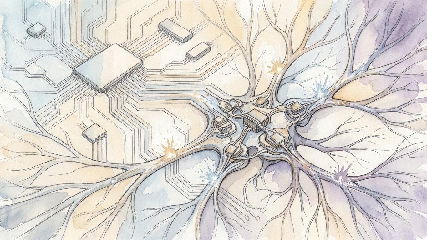
Silicon Synapses – Neuromorphic Chips
For more than seven decades, the exponential march of the digital computer has been dictated by the brilliant architectural blueprint formulated by John von Neumann in 1945: a centralized arithmetic processing unit physically separated from a passive storage memory bank, connected by a narrow electrical bus over which instructions and data must be shuttled sequentially back and forth. In the era of modern artificial intelligence—where multi-billion-parameter neural networks demand continuous, massive matrix multiplications—this separation has collided with an immovable thermodynamic barrier known as the ‘von Neumann bottleneck.’ Modern supercomputers and high-power GPU clusters consume tens of megawatts of electrical power, generating torrents of waste heat simply moving numbers between silicon memory chips and compute cores. In stark, humbling contrast, the human brain performs real-time sensory perception, motor control, abstract reasoning, and continuous lifelong learning on a frugal metabolic power budget of approximately twenty watts—barely enough electricity to illuminate a dim incandescent light bulb. Neuromorphic computing represents a radical departure from digital orthodoxy: the deliberate re-engineering of silicon hardware to emulate the biophysical, event-driven, massively parallel, and co-located architecture of biological nervous systems. By replacing global clock cycles with asynchronous electrical spikes, combining memory and compute into non-volatile synaptic crossbars, and implementing Spiking Neural Networks (SNNs) in analog, digital, and memristive substrates, neuromorphic engineering is forging a new computational paradigm that promises to collapse power consumption by orders of magnitude and bring brain-like intelligence to the edge of the physical world.
1. The Thermodynamic Crisis – The von Neumann Memory Wall
To understand why computer scientists are turning to biological neurobiology, one must first examine the physics of modern digital computing. Since the commercialization of the microprocessor in the early 1970s, performance scaling followed two famous empirical laws: Moore’s Law (the doubling of transistor density per chip every eighteen to twenty-four months) and Dennard Scaling (the physical principle that as transistors shrink, their power density remains constant because operating voltage and capacitance scale down proportionally).
In the mid-2000s, Dennard Scaling died. As transistor gate oxide thicknesses approached the scale of a few nanometers (just a few atomic layers of silicon dioxide), quantum mechanical tunneling of electrons across the gate dielectric caused passive leakage currents to explode. Microprocessor clock frequencies, which had soared from a few megahertz to nearly 4 gigahertz, stalled abruptly: running chips any faster would melt the silicon package. The semiconductor industry pivoted to multicore architectures—packing dozens of parallel cores onto a single die. Yet, multicore scaling could not escape the fundamental thermodynamic trap: The von Neumann Bottleneck.
In a classical computing architecture, arithmetic logic units (ALUs) execute calculations in picoseconds, consuming mere femtojoules of electrical energy. However, the data required for those calculations resides in external Dynamic Random-Access Memory (DRAM). To fetch a single 64-bit floating-point number across a printed circuit board copper trace from an off-chip DRAM chip into the CPU’s register file consumes approximately 100 to 1,000 picojoules of energy—roughly three orders of magnitude more energy than the computation itself! Modern deep learning workloads—such as multiplying massive weight matrices in large language models—are fundamentally memory-bandwidth and energy-bound: high-performance computing clusters spend more than 80% to 90% of their total electrical energy budget simply shuttling weights across buses, fighting the relentless friction of capacitive wire charging.
2. The Biological Miracle – Twenty Watts of Wetware
While an AI datacenter requires its own dedicated electrical substation and gigawatt-scale cooling towers, biological evolution solved this computational challenge hundreds of millions of years ago. The adult human brain contains approximately 86 billion neurons, each connected to an average of 1,000 to 10,000 neighboring cells via specialized junctions called synapses, yielding an astronomical network of over 100 trillion synaptic connections.
Operating inside a warm, fluid-filled cranial vault, the human brain executes real-time 3D stereoscopic vision, continuous auditory scene parsing, dynamic bipedal motor locomotion, emotional inference, language comprehension, and lifelong learning on a continuous power budget of approximately 20 watts. The brain’s computational energy efficiency exceeds that of the world’s most advanced supercomputers by more than six orders of magnitude.
How does biological ‘wetware’ achieve this staggering thermodynamic supremacy? The brain’s architecture violates every single principle of classical von Neumann computing:
- Co-location of Memory and Compute: In the brain, there is no separation between the processor and the hard drive. A synapse is simultaneously a non-volatile memory store (encoding connection strength via receptor density and dendritic spine morphology) and a local computational processor (regulating post-synaptic current flux). Memory and compute are structurally indivisible.
- Massive Asynchronous Parallelism: The brain operates without a centralized, gigahertz master clock. Neurons compute in parallel at biological timescales (milliseconds), operating asynchronously and autonomously.
- Sparse, Event-Driven Communication: Digital computers constantly cycle at billions of Hertz, burning power even when processing redundant or static data. Biological neurons communicate via discrete, all-or-none electrical pulses called Action Potentials (Spikes). If there is no new information, a neuron remains silent, consuming virtually zero dynamic power. At any given moment, less than 1% to 2% of the brain’s neurons are actively firing. Computation is strictly event-driven.
- Analog Computation with Digital Communication: Inside the neuronal dendritic tree and soma, information integration—ionic diffusion, membrane capacitance charging, and temporal summation—is fundamentally analog and continuous. But when the integrated voltage exceeds a threshold, it fires a digital, discrete spike across the axon, providing noise immunity and lossless transmission across long distances.
3. Carver Mead and the Birth of Neuromorphic Engineering
The vision of translating these biological principles into silicon was born in the late 1980s at the California Institute of Technology (Caltech), spearheaded by the legendary microelectronics pioneer Carver Mead. Mead, who had co-authored the foundational textbook Introduction to VLSI Systems with Lynn Conway and coined the term ‘Moore’s Law,’ was struck by a profound physical realization: the physics of semiconductor devices and the biophysics of biological cell membranes are governed by the exact same Boltzmann thermodynamics.
In a standard digital CMOS circuit, Metal-Oxide-Semiconductor Field-Effect Transistors (MOSFETs) are operated as saturated digital switches: the gate voltage is driven well above the threshold voltage (V_th) to turn the transistor fully ‘on,’ maximizing current and speed. Mead recognized that when a MOSFET is operated in its subthreshold or weak-inversion regime (where the gate voltage is below V_th), the channel current does not drop to zero. Instead, current flows via the thermal diffusion of electrons across an energy barrier, following an exponential relationship with gate voltage:
In the subthreshold regime, the drain-source current scales exponentially with gate voltage, mimicking the Boltzmann thermodynamics governing ion diffusion across biological cell membranes.
This exponential voltage-current characteristic is mathematically identical to the exponential Boltzmann behavior that governs the opening and closing of voltage-gated ion channels in biological neuronal membranes, as formulated by Alan Hodgkin and Andrew Huxley! In 1990, Mead published his seminal paper in the Proceedings of the IEEE: “Neuromorphic Electronic Systems,” introducing the word Neuromorphic to the scientific lexicon.
Mead demonstrated that by operating silicon transistors in the subthreshold analog regime, an analog circuit of just a few transistors could directly model the complex, continuous biophysical dynamics of an entire biological synapse or photoreceptor while consuming mere picowatts or femtowatts of power. Working with Misha Mahowald, Mead constructed the world’s first silicon retina—an analog chip that emulated the spatial and temporal processing of biological retinal cones, horizontal cells, and bipolar cells, capturing visual motion directly in hardware.
4. The Mathematical Foundation – Spiking Neural Networks (SNNs)
To program neuromorphic hardware, computer scientists developed the theoretical framework of Spiking Neural Networks (SNNs), often described as the ‘third generation’ of artificial neural networks. Unlike first-generation networks (perceptrons with binary threshold outputs) and second-generation networks (standard deep learning models where neurons output continuous real numbers via activation functions like ReLU or sigmoid), SNNs communicate strictly through discrete temporal events: spikes.
The Leaky Integrate-and-Fire (LIF) Model
The standard mathematical workhorse of neuromorphic computing is the Leaky Integrate-and-Fire (LIF) neuron model. A LIF neuron treats the neuronal plasma membrane as a parallel electrical circuit composed of a membrane capacitance C_m and a passive leak resistance R_m, driven by incoming synaptic currents I_syn(t):
In a leaky integrate-and-fire model, incoming synaptic currents continuously charge the neuron’s membrane capacitance, while an intrinsic leak resistance pulls the voltage back toward its resting potential over a timescale of ten to twenty milliseconds.
The dynamics unfold with temporal elegance: 1. Integration: When incoming spikes arrive at post-synaptic terminals, they inject discrete packets of charge, incrementally charging the membrane capacitor V(t). 2. Leakage: If no further spikes arrive, the membrane potential continuously decays exponentially back toward V_rest via the leak resistor, implementing a natural temporal decay that forgets stale information. 3. Threshold Firing: If incoming spikes arrive in close temporal proximity, their charges summate. When the membrane potential crosses a critical threshold voltage V_th, the neuron instantly fires a discrete output spike: S(t) = delta(t – t_spike). 4. Reset and Refractory Period: Immediately upon firing, the membrane potential is instantaneously reset to a hyperpolarized potential V_reset, where it is clamped for an absolute refractory period of a few milliseconds, during which the neuron cannot fire again.
In an SNN, information is not encoded merely in the static magnitude of a scalar value; it is encoded in the rich temporal domain: in the Inter-Spike Interval (ISI), in the precise phase of firing relative to an oscillation, or in the precise temporal latency of the very first spike following a stimulus.
5. Synaptic Plasticity – Learning in Silicon via STDP
How does a neuromorphic network learn without a centralized backpropagation algorithm? In biological neurobiology, learning is governed by local synaptic plasticity rules, first postulated by Donald Hebb in 1949: “Neurons that fire together, wire together.”
In the late 1990s, Henry Markram, Guo-qiang Bi, and Mu-ming Poo discovered the precise biophysical rule that governs this adaptation: Spike-Timing-Dependent Plasticity (STDP). STDP is a temporally asymmetric form of Hebbian learning driven by the precise microsecond-level timing difference (the relative timing between pre- and post-synaptic spikes) between the arrival of a pre-synaptic action potential and the firing of the post-synaptic neuron:
- Long-Term Potentiation (LTP / Synaptic Strengthening): If the pre-synaptic neuron fires a spike immediately before the post-synaptic neuron fires (delta t > 0, typically within 20 milliseconds), the pre-synaptic neuron contributed to causing the post-synaptic event. The synapse strengthens: its synaptic weight potentiates exponentially as the time interval between spikes narrows.
- Long-Term Depression (LTD / Synaptic Weakening): Conversely, if the pre-synaptic neuron fires immediately after the post-synaptic neuron has already fired (delta t < 0), the pre-synaptic spike was un-correlated with the firing event. The synapse weakens: its weight depresses exponentially as the negative timing delay increases.
STDP is an inherently local, unsupervised learning rule: it requires only the physical electrical signals present at that specific local synapse at that specific millisecond. It requires zero global backpropagation passes, zero non-local memory reads, and zero centralized oversight, enabling neuromorphic silicon to learn autonomously in real time directly from streaming sensory environments.
6. The Digital Neuromorphic Titans – IBM TrueNorth and Intel Loihi
While Carver Mead pioneered analog neuromorphic circuits, early analog systems were notoriously sensitive to thermal drift, semiconductor process variations, and electrical noise. To achieve industrial reliability, leading semiconductor corporations engineered fully digital neuromorphic architectures that preserve the event-driven, spiking mathematics of neurobiology within reliable digital CMOS logic.
IBM TrueNorth (2014)
Developed under the DARPA SyNAPSE program by Dharmendra Modha and IBM Research, TrueNorth was the first monolithic neuromorphic supercomputing chip. Fabricated on a 28-nanometer process, TrueNorth integrated 5.4 billion transistors across a 2D mesh of 4,096 parallel neurosynaptic cores. The single chip emulated 1 million digital spiking neurons and 256 million programmable synapses.
TrueNorth was fully asynchronous: it contained zero global clock distribution networks. Cores communicated via a 2D on-chip mesh network-on-chip (NoC) using Address-Event Representation (AER) packets. When operating at peak biological capacity, TrueNorth consumed a mere 70 milliwatts of electrical power—a power density so low that the chip could run on a hearing-aid battery and was cool to the touch, operating four orders of magnitude more efficiently than conventional CPU architectures on visual pattern recognition tasks.
Intel Loihi and Loihi 2 (2017–2021)
In 2017, Mike Davies and Intel Labs unveiled Loihi, an advanced asynchronous digital neuromorphic processor fabricated on Intel’s 14-nm FinFET process, followed in 2021 by Loihi 2 on the Intel 4 process. Unlike TrueNorth’s fixed, hardwired leaky integrate-and-fire model, Loihi was engineered for on-chip programmable learning.
Each Loihi chip integrates 128 neuromorphic cores, accommodating up to 131,072 neurons and 130 million synapses, alongside three embedded asynchronous x86 processor cores for input/output management. Loihi features a fully programmable microcode learning engine: software developers can program custom mathematical plasticity rules—including generalized STDP, three-factor reinforcement learning rules (combining pre- and post-synaptic spikes with a neuromodulatory dopamine reward signal), and associative memory recall.
When evaluated on complex computational problems—such as real-time visual gesture recognition, robotic arm path planning, graph optimization, and sparse database search—Loihi demonstrated up to 1,000 times greater energy efficiency and 100 times lower latency than modern GPUs, proving that asynchronous digital spiking silicon can conquer real-time edge computing.
7. Memristors and Phase-Change Memory – The In-Memory Computing Frontier
While digital neuromorphic chips like Loihi achieve extraordinary efficiency, they still construct neurons and synapses out of dozens of digital CMOS transistors and SRAM cells, consuming significant silicon die area. The ultimate physical manifestation of neuromorphic engineering is In-Memory Analog Computing via Memristive Crossbars.
In 1971, the non-linear circuit theorist Leon Chua at UC Berkeley predicted the existence of a fourth fundamental passive two-terminal electrical circuit element (joining the resistor, capacitor, and inductor): the Memristor (Memory-Resistor). Chua mathematically proved that there must exist an element that establishes a functional relationship between magnetic flux and electric charge, exhibiting a resistance that dynamically changes based on the history of electrical current that has passed through it.
In 2008, Stanley Williams and his team at HP Labs announced the physical realization of a nanoscale titanium dioxide (TiO_2) memristor. Today, memristive technology has expanded into a rich family of non-volatile analog memory devices: – Phase-Change Memory (PCM): Utilizing chalcogenide glass materials (such as Ge_2Sb_2Te_5, GST). Applying electrical heating pulses reversibly switches the material between an amorphous state (high electrical resistance) and a crystalline state (low electrical resistance), providing continuous analog conductance states. – Resistive RAM (RRAM / ReRAM): Utilizing transition metal oxides (HfO_x, TaO_x). Electric fields drive the migration of oxygen vacancies, forming and dissolving nanoscale metallic conductive filaments that modulate electrical conductance. – Magnetic RAM (MRAM) and Spintronic Synapses: Utilizing spin-transfer torque (STT) and spin-orbit torque (SOT) to modulate the magnetic orientation of ferromagnetic layers across a magnetic tunnel junction (MTJ).
The Magic of the Crossbar Array
When memristors are arranged in a 2D crossbar grid—where rows serve as input word-lines and columns serve as output bit-lines—they execute the fundamental mathematical operation of artificial intelligence (Matrix-Vector Multiplication, y = A · x) entirely in the analog physical domain at the speed of light!
The physics is breathtakingly simple: 1. Input vector components x_i are encoded as analog voltages V_i applied to the horizontal rows. 2. The matrix weights A_ij are encoded directly as the physical conductances G_ij of the memristors located at the crossbar intersections. 3. According to Ohm’s Law, the current flowing through each memristor is the physical product of input voltage and device conductance. 4. According to Kirchhoff’s Current Law, currents flowing down each vertical wire sum together automatically at the speed of light, performing continuous vector-matrix multiplication with zero digital clock cycles.
The entire matrix multiplication is executed in a single physical clock cycle with zero memory movement! The computation is performed directly inside the memory itself (In-Memory Computing). A memristive crossbar can execute petascale matrix multiplications consuming mere milliwatts of electrical power, operating as the closest physical approximation of biological synaptic neuropil ever manufactured by human hands.
8. Event-Based Sensing – Neuromorphic Dynamic Vision Sensors (DVS)
A brain-inspired processor is fundamentally mismatched if it is fed data from traditional digital sensors. Conventional digital video cameras operate on an archaic, artificial paradigm: the Frame Rate. Every 33 milliseconds (30 frames per second), a conventional camera reads out every single pixel in its sensor array, regardless of whether anything changed in the scene. If a camera stares at an empty wall, it generates millions of redundant pixels per second, flooding communication buses and consuming immense processing power.
To provide true neuromorphic input, pioneers—led by Tobi Delbruck at ETH Zurich and the University of Zurich—invented Event-Based Cameras, specifically the Dynamic Vision Sensor (DVS). The DVS abandons the concept of frames entirely.
In a DVS pixel array, each individual photodiode pixel operates completely autonomously and asynchronously. The pixel circuitry contains a logarithmic photoreceptor and an analog differential circuit that continuously monitors the local light intensity. The pixel remains completely silent until the relative change in logarithmic illumination exceeds a predetermined threshold:
The instant this threshold is crossed, the individual pixel immediately emits an asynchronous digital event packet containing its (X, Y) coordinate, an exact microsecond timestamp, and a binary polarity (+1 for brightening, -1 for dimming). If nothing moves in the scene, the camera transmits zero bytes of data and consumes zero dynamic power. If a high-speed bullet or bird crosses the field of view, only the pixels tracing the edge of the moving object fire events.
The performance metrics of event cameras are extraordinary: – Microsecond Temporal Resolution: Equivalent to a conventional high-speed camera operating at 10,000 to 100,000 frames per second, with zero motion blur. – Massive Dynamic Range: Exceeding 120 to 140 decibels (compared to 60 dB for standard cameras), allowing an event camera to simultaneously capture details inside a pitch-black tunnel while looking directly into the midday sun. – Ultra-Low Data Bandwidth and Power: Consuming milliwatts of power and generating kilobytes of data rather than gigabytes.
When paired directly with a neuromorphic spiking processor like Loihi or an SNN edge chip, event cameras enable autonomous drones to dodge high-speed obstacles in milliseconds, satellite tracking systems to detect hypersonic debris, and robotic grippers to grasp fast-moving objects with biological agility.
9. The Algorithmic Dilemma – Training SNNs and Surrogate Gradients
While neuromorphic hardware has demonstrated miraculous efficiency, the entire field was long held back by a formidable mathematical roadblock: How do you train a Spiking Neural Network?
Modern deep learning owes its global triumph to Backpropagation and Stochastic Gradient Descent (SGD). Backpropagation relies on the chain rule of differential calculus, which requires that every mathematical operation in the neural network must be continuous and differentiable (having a well-defined first derivative).
In a biological spiking neuron, the output activation is a discrete Heaviside Step Function: the neuron outputs a zero if the membrane potential is below threshold, and fires an instantaneous Dirac delta spike (delta(t)) the instant it crosses threshold. The mathematical derivative of a step function is pathological: it is zero everywhere, and explodes to infinity (infty) at the exact threshold boundary:
Because the biological spike threshold acts as an abrupt step function, its mathematical derivative is zero everywhere except at the threshold, where it shoots to infinity. To train spiking networks with backpropagation, researchers replace this non-differentiable jump with a smooth surrogate gradient during learning.
If you attempt to apply standard backpropagation to an SNN, the error gradients either vanish to zero or explode to infinity; the network cannot learn. For years, researchers were forced to use crude workarounds: training a standard non-spiking ANN (with ReLU activations) and then mathematically converting the trained weights into an SNN. While effective for simple vision tasks, converted SNNs suffered high latency and lost the unique temporal dynamics of true biological spiking.
The breakthrough arrived in the late 2010s with the invention of Surrogate Gradient Learning, pioneered by Emre Neftci, Friedemann Zenke, and Suraj Gowda. In surrogate gradient training: – In the Forward Pass, the network executes true, discrete, non-differentiable spiking dynamics: neurons integrate charge and emit physical binary spikes. – In the Backward Pass, the non-differentiable Dirac delta derivative is replaced by a smooth, continuous surrogate mathematical function—such as the derivative of a fast sigmoid, an arctangent, or a triangular function.
Surrogate gradients unlocked the ability to train deep Spiking Neural Networks directly from scratch using standard deep learning frameworks like PyTorch and JAX (via libraries such as SpikingJelly and snnTorch). Today, SNNs trained with surrogate gradients achieve state-of-the-art accuracy on speech recognition, video gesture classification, and radar tracking benchmarks while preserving the ultra-low-power, event-driven advantages of neuromorphic silicon.
10. Real-World Applications – From Acoustic Edge to Deep Space
The commercial and scientific deployment of neuromorphic systems is accelerating rapidly across domains where electrical power is scarce, latency is critical, and operational environments are harsh:
- Ultra-Low-Power Edge Acoustic Sensing: In voice-activated consumer devices (smartphones, earbuds), traditional processors burn battery life continuously listening for wake words like ‘Hey Siri’ or ‘Alexa.’ Neuromorphic auditory chips—such as SynSense’s Speck or GrAI Matter Labs processors—utilize silicon cochlea architectures that process acoustic frequency channels as asynchronous spikes, consuming less than 1 milliwatt in continuous listening mode.
- Extreme Neuromorphic Robotics: Quadcopter drones operating in dense forests or GPS-denied environments require millisecond visual-motor reaction times. By pairing an event camera with an SNN running on Loihi, roboticists at TU Delft achieved autonomous high-speed drone racing and obstacle avoidance at velocities exceeding 10 meters per second, operating with a reaction latency of less than 3 milliseconds.
- Deep Space Exploration and Hypersonic Tracking: In deep space satellites, radiation tolerance and extreme power constraints are paramount. Neuromorphic event sensors deployed by the United States Air Force and international space agencies continuously track orbital space debris and satellites in geostationary orbit without blinding sensor bloom, consuming a fraction of the mass, volume, and solar panel power of traditional optical telescopes.
- Brain-Machine Interfacing: Intracortical BCI implants (such as those developed by Neuralink or BrainGate) can embed neuromorphic spiking processors directly within the hermetic cranial titanium enclosure. By processing neural spikes using on-chip spiking neural networks, the implant decodes motor intent locally, slashing radio telemetry bandwidth and keeping thermal dissipation well below safety limits.
12. Massively Parallel Cortical Emulation – The SpiNNaker Architecture
While neuromorphic chips like TrueNorth and Loihi pursued custom digital hardware accelerators, a radically different philosophical approach to brain simulation was pioneered by Steve Furber at the University of Manchester. Furber—who in the early 1980s had co-designed the revolutionary BBC Micro and the original 32-bit ARM microprocessor architecture (which now powers virtually every smartphone on Earth)—turned his engineering genius toward constructing the world’s largest biological neural network simulator: SpiNNaker (Spiking Neural Network Architecture).
Furber asked: Instead of designing custom, un-programmable analog circuits or rigid neuromorphic ASICs, can we construct a supercomputer out of millions of ultra-low-power, general-purpose embedded ARM processor cores, bound together by an unprecedented, biologically inspired communications fabric?
Completed in 2018 under the European Union Human Brain Project, the flagship SpiNNaker machine is an engineering colossus: – One Million ARM Cores: Comprising 57,600 custom packaging nodes, each containing eighteen ARM968 processor cores paired with a synchronous dynamic RAM (SDRAM) die via system-in-package (SiP) wire bonding, yielding 1,036,800 active 32-bit processing cores. – The Self-Routing Multicast Fabric: The defining innovation of SpiNNaker is its communication router. In a biological brain, a single pyramidal neuron projects an axon that branches into thousands of terminal arborizations, broadcasting its action potential simultaneously to thousands of post-synaptic targets. In a standard supercomputer, point-to-point packet routing would instantly collapse under billions of simultaneous spike messages. Furber’s team engineered a custom hardware Multicast Router in each chip connected in a hexagonal 2D toroidal mesh topology.
When an ARM core simulates a neuron that fires a spike, it generates an un-routed, tiny 32-bit Address-Event packet containing only the originating neuron’s ID. As this packet traverses the network, each node’s multicast router matches the ID against a local, associative ternary Content-Addressable Memory (TCAM) routing table. If the router finds a match, it instantaneously replicates the packet, transmitting it out through multiple physical link directions simultaneously while dropping local copies into its own on-chip ARM cores. The network handles over one billion discrete spikes per second with zero packet buffer congestion and sub-millisecond latencies, simulating large-scale cortical columns, basal ganglia loops, and cerebellar circuits in biological real time.
13. Accelerated Physical-Model Neuromorphic Systems – BrainScaleS
While SpiNNaker and Loihi operate in biological real time (where one millisecond in reality equals one millisecond in simulation), an entirely different domain of neuromorphic engineering was pioneered by the late Karlheinz Meier and his team at Heidelberg University: Accelerated Analog Neuromorphic Computing, embodied in the BrainScaleS project.
Meier recognized that while biological neurons operate at the slow speed of chemical diffusion across aqueous ion channels (milliseconds), silicon transistors switch at the speed of electromagnetic fields (nanoseconds). Why force silicon to operate at the sluggish pace of biology? BrainScaleS implements Physical-Model Analog Neuromorphic Circuits operating at an acceleration factor of ten thousand times faster than biological real time!
In the BrainScaleS architecture, circuits do not numerically solve differential equations through mathematical software loops. Instead, the silicon circuits are the physical embodiment of the equations! Miniature analog circuits—utilizing operational transconductance amplifiers (OTAs), capacitors, and resistors—physically emulate the continuous non-linear membrane conductance dynamics of the Adaptive Exponential Integrate-and-Fire (AdEx) biological neuron model.
Operating on an entire unbroken 200-millimeter silicon wafer (Wafer-Scale Integration), BrainScaleS integrates 384 High-Count analog Reticle blocks, containing 180,000 neurons and 40 million programmable analog synapses per wafer. Because the system runs 10,000 times faster than nature, an entire biological day of neural learning and adaptation (86,400 seconds) is executed in just 8.6 seconds of physical wall-clock time! This breathtaking speed acceleration allows neuroscientists to simulate weeks of developmental synaptic plasticity, long-term memory consolidation, and evolutionary adaptation in minutes, while reducing the energy consumption per simulated synaptic event to mere picojoules.
14. Probabilistic Computing with Stochastic Spintronics and p-Bits
As neuromorphic engineering converges with quantum mechanics, physicists are harnessing a physical property that traditional digital computer engineers spent decades trying to suppress: Thermal Noise and Device Stochasticity.
In standard digital logic, a bit must be deterministically zero or one; thermal noise that causes a bit to flip randomly is a catastrophic hardware error. In biological neurobiology, however, synapses and ion channels are inherently noisy and stochastic: when an action potential arrives at a pre-synaptic terminal, the probability that a synaptic vesicle will actually fuse and release neurotransmitter is often less than 20% to 50%! Nature uses thermodynamic stochasticity as a computational asset to escape local energy minima, perform Bayesian probabilistic inference, and sample from complex probability distributions.
In the late 2010s, Supriyo Datta at Purdue University and researchers at Tohoku University introduced Probabilistic Bits (p-bits) using Stochastic Magnetic Tunnel Junctions (s-MTJs). A magnetic tunnel junction consists of two ferromagnetic layers separated by an ultra-thin insulating dielectric barrier. In standard non-volatile MRAM, the magnetic free layer is engineered with high energy barriers to remain stable for ten years. In an s-MTJ, the energy barrier is intentionally lowered to match the thermal energy of the room (E_B approximately k_B T).
Under continuous thermal bombardment, the magnetization of the free layer fluctuates spontaneously and continuously, flipping between parallel (low resistance) and anti-parallel (high resistance) states at gigahertz frequencies. By applying a tiny input bias current, the probability of the p-bit dwelling in state +1 versus -1 can be smoothly and continuously tuned according to the classical Boltzmann sigmoid function.
When networks of these stochastic spintronic p-bits are interconnected via resistive crossbars, they form physical Boltzmann Machines. These probabilistic neuromorphic networks solve intractable NP-hard combinatorial optimization problems—such as the Traveling Salesperson Problem, boolean satisfiability, integer factorization, and graph partitioning—by naturally exploring the combinatorial solution space through physical thermodynamic annealing, arriving at optimal global solutions orders of magnitude faster than classical simulated annealing algorithms on supercomputers.
15. Neuromorphic Olfaction – The Electronic Nose of the Mammalian Bulb
Perhaps the most dazzling biological demonstration of neuromorphic capability occurred when neurophysiologists and microchip designers teamed up to solve the hardest problem in sensory biology: Chemical Olfaction.
While computer vision and audio speech processing have advanced rapidly, artificial ‘electronic noses’ have lagged severely behind. Traditional gas chromatography and mass spectrometry systems are bulky, slow, and consume hundreds of watts. In 2020, Thomas Cleland at Cornell University and Mike Davies at Intel Labs programmed the Loihi neuromorphic processor to emulate the biological circuitry of the mammalian Olfactory Bulb.
The mammalian olfactory system is an evolutionary marvel: an animal can sniff an environment flooded with thousands of competing background scents (diesel exhaust, humidity, vegetation) and instantly identify a single, faint whiff of a dangerous predator or toxic chemical in a single inhalation, learning to recognize new chemical odorants after only one exposure (one-shot learning).
Cleland and Davies mapped the precise biological microcircuits of the olfactory bulb onto Loihi: 1. Glomerular Layer: 72 chemical chemosensors with broad, overlapping cross-sensitivities recorded electrical resistance changes when exposed to volatile hazardous chemical plumes (including acetone, ammonia, methane, and carbon monoxide). 2. Mitral and Granule Cells: Incoming sensor signals were converted into sparse temporal spike trains. Mitral cells executed mutual lateral inhibition via local inhibitory granule interneurons, driving rapid oscillatory synchronization across the neural population. 3. Spike-Timing Associative Plasticity: When a new chemical was introduced, the phase of action potentials relative to the collective gamma-frequency oscillation (40–80 Hz) modified synaptic weights via spike-timing plasticity, burning the unique multidimensional chemical ‘odor fingerprint’ into the network.
The results were stunning: Loihi learned to identify hazardous chemical plumes with one-shot learning—requiring only a single training exposure, whereas standard deep learning neural networks required thousands of training samples. Furthermore, when the chemical was buried in dense, overwhelming background interference (simulating real-world industrial chemical leaks or airport explosives detection), Loihi identified the target chemical with 92% accuracy, outperforming conventional deep learning models while consuming less than a few milliwatts of electrical power.
16. Bio-Signal Neuromorphic Edge Implants – Ultra-Low-Power Medicine
One of the most immediate and life-saving applications of neuromorphic computing is the creation of intelligent, autonomous medical implants that operate directly inside the human body. Traditional biomedical implants—such as cardiac pacemakers, implantable cardioverter-defibrillators (ICDs), and deep brain stimulators—rely on rigid, handcrafted heuristic algorithms (such as threshold voltage crossing) to detect cardiac arrhythmias or epileptic seizures.
If clinicians attempt to deploy modern deep learning algorithms (such as convolutional neural networks) on implantable devices to improve diagnostic accuracy, the battery of the implant is depleted within weeks due to the continuous high-power consumption of digital microcontrollers. A patient would require repeated, invasive surgical operations simply to replace depleted batteries.
Neuromorphic engineering solves this medical dilemma by deploying sub-microwatt Analog Neuromorphic Front-Ends paired with on-chip Spiking Neural Networks: – Neuromorphic Electrocardiogram (ECG) Classifiers: Pioneered by Giacomo Indiveri at the Institute of Neuroinformatics (INI) in Zurich, tiny analog neuromorphic chips continuously monitor cardiac electrical rhythms. Incoming analog ECG signals are converted into asynchronous temporal spike trains by an array of analog integrate-and-fire circuits. An on-chip SNN trained via surrogate gradients continuously classifies heartbeats—distinguishing normal sinus rhythms from lethal ventricular fibrillation and atrial flutter in real time—while consuming less than 500 nanowatts of continuous power! Powered purely by energy harvested from body heat (thermoelectric generators) or arterial blood pressure pulsations, a neuromorphic cardiac monitor can operate perpetually without ever needing a battery replacement. – Neuromorphic Electromyography (EMG) for Bionic Limbs: Prosthetic robotic arms require continuous decoding of muscle signals from the user’s residual limb. Neuromorphic processors directly process the sparse, bursting spike trains of motor unit action potentials (MUAPs) recorded from surface EMG electrodes, predicting intended hand gestures (pinch, grasp, point) with latency below 5 milliseconds and power consumption low enough to embed inside the prosthetic hand’s carbon-fiber socket.
17. The Philosophical Horizon – The Physics of Thought
The philosophical implications of neuromorphic engineering reach into the deepest questions of cognitive philosophy and the mind-body problem. For decades, the dominant paradigm in artificial intelligence was Computational Functionalism—the view, articulated by Alan Turing and Hilary Putnam, that intelligence is fundamentally substrate-independent software. Under functionalism, it does not matter whether an algorithm executes on carbon-based neurons, silicon microprocessors, or vacuum tubes: as long as the formal logical program is executed, the mind is achieved.
Neuromorphic computing challenges this substrate-agnostic dogma by asserting that Physics Matters. Biological cognition is not an abstract, detached mathematical program running on a generic, passive calculating machine; cognition is an emergent physical property of a specific, non-equilibrium thermodynamic system. The time delays of axonal conduction, the thermal noise of ion channels, the analog integration of charge across lipid membranes, and the spatial morphology of dendritic trees are not incidental imperfections of biological evolution—they are the essential physical constraints that make real-time, low-power adaptive intelligence possible!
By building physical systems where memory and computation are indivisible, where time is its own representation, and where information is communicated through the sparse, asynchronous choreography of spikes, neuromorphic engineers are proving that we cannot separate the mind from the physical architecture of the brain. Carver Mead’s timeless insight—that silicon can be operated according to the exact same thermodynamic principles that govern living tissue—has closed the conceptual divide between the machine and the organism.
11. Conclusion – The Neuromorphic Horizon
The journey of neuromorphic computing—from Carver Mead’s visionary analog silicon retinas in 1990, to IBM TrueNorth’s asynchronous million-neuron mesh, to Intel Loihi’s programmable plasticity, memristive crossbar accelerators, and event-based dynamic vision sensors—marks one of the most sublime intellectual migrations in the history of engineering. It represents the ultimate humbling and uplifting of computer science: the recognition that after seventy years of digital dominance, nature’s four-billion-year-old biological design remains the supreme computational benchmark.
Neuromorphic engineering is not merely an incremental optimization of existing microprocessors; it is a foundational paradigm shift. By tearing down the physical wall between memory and computation, discarding the tyrannical tick of the global clock, and embracing the sparse, event-driven elegance of the electrical spike, neuromorphic engineering has unlocked an extraordinary computational future.
As we stand on the threshold of an interconnected world of billions of autonomous edge devices, medical implants, and robotic systems, the twenty-watt miracle of the biological brain is no longer an unapproachable evolutionary mystery. It has become our engineering blueprint. Silicon has learned to speak the language of the synapse, and through that language, the machines of tomorrow will perceive, learn, and reason with the effortless, thermodynamic elegance of life itself.
As we gaze forward into the mid-twenty-first century, the ultimate destiny of artificial intelligence will not be decided solely in hyper-scale cloud datacenters consuming gigawatts of fossil and nuclear power. The true test of intelligent computing will be its ubiquity, its sustainability, and its intimacy with the physical universe. An artificial intelligence that requires an entire electrical power plant to recognize a human face or navigate a vehicle is an evolutionary dead end—a fragile, energy-starved titan that cannot survive outside its climate-controlled sanctuary.
Neuromorphic computing offers a radically different, sustainable evolutionary path. By embodying the sublime physical economy of the mammalian brain in solid-state silicon, neuromorphic systems will enable a world of ambient, distributed intelligence: autonomous environmental monitoring networks that sleep in wilderness forests for decades on solar micropower; intelligent prosthetic limbs that converse directly with peripheral nerves; and robotic explorers that navigate the light-starved canyons of Mars with the split-second reflexes of a dragon-fly.
In the grand history of science, Carver Mead’s revolution will be celebrated as the moment when microelectronics ceased to be merely an arithmetic calculator and became an authentic, living mirror of the nervous system. The silicon synapse has awakened, and through its quiet, event-driven whisper, the future of computing will think with the timeless, twenty-watt brilliance of life itself.
From the delicate analog current mirrors designed in Carver Mead’s Pasadena laboratory to the massive asynchronous neural meshes of Loihi and SpiNNaker, neuromorphic engineering stands as an unshakeable monument to human curiosity and biomimetic mastery. By unifying the laws of solid-state semiconductor physics with the principles of neural computation, science has bridged the chasm between the artificial and the biological, inaugurating an extraordinary era of thermodynamic harmony, cognitive empowerment, and sustainable computing for all humanity.
Through every age of innovation, humanity has sought to understand the nature of its own mind. In building the silicon synapse, we have not only revolutionized technology; we have held up an electronic mirror to the soul of life itself, proving that the spark of thought can be ignited in the quiet physics of the chip.